


The piezoresistive effect is the change of electric resistivity of the material caused by an applied mechanical strain or stress. Many materials change their resistance when strained, but the piezoresistive effect is most pronounced in semiconductors. Semiconductor piezoresistive sensing elements, or piezoresistors, are typically used as pressure and force sensors, where the applied mechanical load is converted into a proportional electric signal. Typical applications of piezoresistors are pressure transducers and accelerometers.
You use piezoresistive analysis to determine the change in electric field or current distributions due to applied forces or pressure. The elements that allow you to do a piezoresistive analysis are:
| PLANE222, KEYOPT(1) = 101 - coupled-field 4-node quadrilateral |
| PLANE223, KEYOPT(1) = 101 - coupled-field 8-node quadrilateral |
| SOLID225, KEYOPT(1) = 101 - coupled-field 8-node brick |
| SOLID226, KEYOPT(1) = 101 - coupled-field 20-node brick |
| SOLID227, KEYOPT(1) = 101 - coupled-field 10-node tetrahedron |
The analysis type can be either steady-state (ANTYPE,0) or transient (ANTYPE,4).
Hints for Performing a Piezoresistive Analysis
At least two iterations are required to calculate the piezoresistive effect.
The force label for the VOLT degree of freedom is AMPS. Use this label in F, CNVTOL, RFORCE, etc.
To do a piezoresistive-circuit analysis, use CIRCU124.
Use the JC label on PRNSOL/PLNSOL, PRESOL/PLESOL, or PRVECT/PLVECT to print or plot conduction current density results.
The following related topics are available:
A piezoresistive analysis requires the specification of electrical resistivity, the elastic coefficients, and the piezoresistive matrix. See the following topics for details:
Specify electrical resistivity values (MP) as RSVX, RSVY, RSVZ ().
To take into account capacitive effects in a transient piezoresitive analysis, you can specify electrical permittivities as PERX, PERY, and PERZ via MP .
Input the elastic coefficient matrix using the data table input (TB,ANEL and TBDATA). See Elastic Coefficient Matrix for a discussion on the elastic coefficient matrix. Alternatively, you can specify Young's modulus (MP,EX) and Poisson's ratio (MP,NUXY). To specify these values via the GUI:
You can specify piezoresistive matrix either in the form of piezoresistive stress matrix [π] or piezoresistive strain matrix [m] (TB,PZRS and TBDATA).
The piezoresistive stress matrix [π] (TBOPT = 0)
uses stress to calculate the change in electric resistivity due to the
piezoresistive effect. The piezoresistive strain matrix [m]
(TBOPT = 1) uses elastic strain to calculate the
change in electric resistivity due to the piezoresistive effect. (See Piezoresistivity in the Theory Reference for more
information.)
In a general case, the piezoresistive matrix is a non-symmetric 6x6 matrix that relates the x, y, z, xy, yz, xz terms of stress or strain to the x, y, z, xy, yz, xz terms of electric resistivity via 36 constants. (See Piezoresistivity in the Material Reference for a description of the matrix used.) For the semiconductor materials (for example, silicon) that belong to the cubic group of symmetry, the piezoresistive matrix has only three independent coefficients, π11, π12, π44:

and [π] can be input as follows:
| TB,PZRS |
| TBDATA,1,π11, π12,π12 |
| TBDATA,7,π12,π11, π12 |
| TBDATA,13,π12,π12,π11 |
| TBDATA,22,π44 |
| TBDATA,29,π44 |
| TBDATA,36,π44 |
To define the piezoresistive matrix via the GUI, use the following:
Define data in consistent units. When modeling micro-electromechanical systems (MEMS), it is best to use μMKSV or μMSVfA units (see Table 1.8: Piezoresistive Conversion Factors for MKS to μMKSV and Table 1.15: Piezoresistive Conversion Factors for MKS to μMKSVfA).
This example problem considers a piezoresistive four-terminal sensing element described in M.-H. Bao, W.-J. Qi, Y. Wang, "Geometric Design Rules of Four-Terminal Gauge for Pressure Sensors", Sensors and Actuators, 18 (1989), pp. 149-156.
The following topics are available:
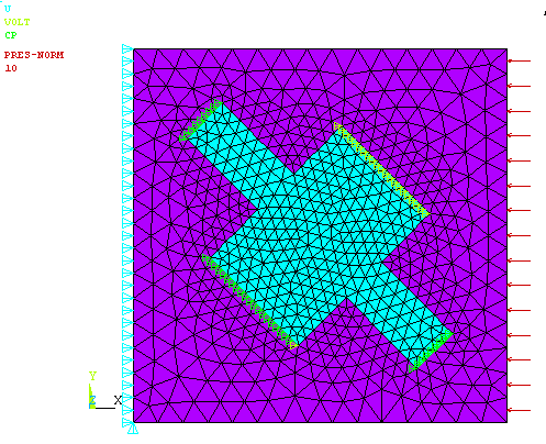
The sensing element consists of a rectangular p-type piezoresistor diffused on an n-type silicon diaphragm. The length of the diaphragm is oriented along the crystallographic direction X || [110] of silicon. The piezoresistor is a rectangular plate of length L and width W with two current contacts located at the ends of the plate. For maximum stress sensitivity, the piezoresistor is oriented at a 45° angle to the sides of the diaphragm. A supply voltage Vs is applied to the electrodes to produce a current in the length direction of the plate. The stress in the resistor material caused by pressure p on the diaphragm generates a proportional transverse electric field in the width direction. The output voltage Vo induced by this field is extracted from the two signal-conducting arms of length a and width b.

Perform a 2D static piezoresistive analysis to determine the output voltage Vo of the sensing element.
Material and geometric properties are input in the μMKSV system of units. For more information on units, see System of Units.
The material properties for silicon (Si) are:
| Si stiffness coefficients, MN/m2: |
| c11 = 165.7e3 |
| c12 = 63.9e3 |
| c44 = 79.6e3 |
| p-type Si resistivity = 7.8e-8 T Ωµm |
| p-type Si piezoresistive coefficients, (MPa)-1: |
| π11 = 6.5e-5 |
| π12 = -1.1e-5 |
| π44 = 138.1e-5 |
The geometric parameters are:
| Width of piezoresistor (W) = 57 μm |
| Length of piezoresistor (L) = 1.5W |
| Width of signal-conducting arm (b) = 23 μm |
| Length of signal-conducting arm (a) = 2b |
| Size of the square diaphragm (S) = 2L |
Loading for this model is:
| Supply voltage (Vs) = 5 V |
| Pressure on the diaphragm (p) that creates stress in the X direction (Sx)= -10 MPa |
A series of 2D piezoresistive static analyses was performed to determine the output voltage Vo of the sensing element as a function of its geometrical dimensions. Results are compared to the analytical solution given by:

which gives a good approximation of the transverse voltage for ideal geometries (that is, when L is much larger than W, and the configuration has no signal-conducting arms and output contacts).
Table 2.21: Sensing Element Output Voltage
| L/W | Vo, mV (Results) | Vo, mV (Analytical Results) |
|---|---|---|
| 1.25 | 25.9 | 27.6 |
| 1.5 | 23.1 | 23.0 |
| 2.0 | 18.4 | 17.3 |
| 2.5 | 15.5 | 13.8 |
| 3.0 | 12.8 | 11.5 |
/batch,list
/title, Four-terminal piezoresistive element, uMKSV system of units
/com,
/com,  Geometric parameters:
/com,
W=57                          ! width of piezoresistor, um
L=1.5*W                       ! length of piezoresistor, um
b=23                          ! width of signal-conducting arm, um
a=2*b                         ! length of signal-conducting arm, um
S=2*L                         ! size of square diaphragm, um
/com,
/com,  Material properties (Si):
/com,
/com,  Stiffness,  MN/m^2
/com,   [c11 c12 c12  0 ]
/com,   [c12 c11 c12  0 ]
/com,   [c12 c12 c11  0 ]
/com,   [ 0   0   0  c44]
/com,
c11= 16.57e4
c12= 6.39e4
c44= 7.96e4
/com,
/com,  Resistivity (p-type Si), TOhm*um
rho= 7.8e-8
/com,
/com,  Piezoresistive coefficients (p-type Si), (MPa)^(-1)
/com,   [p11 p12 p12  0 ]
/com,   [p12 p11 p12  0 ]
/com,   [p12 p12 p11  0 ]
/com,   [ 0   0   0  p44]
/com,
p11=6.5e-5
p12=-1.1e-5
p44=138.1e-5
/com,
/com,  Pressure load, MPa
p=10
/com,  Source voltage, Volt
Vs=5
/nopr

/prep7
et,1,PLANE223,101            ! piezoresistive element type, plane stress
et,2,PLANE183                ! structural element type, plane stress

                             ! Specify material orientation
local,11
local,12,,,,,45              ! X-axis along [110] direction

                             ! Specify material properties:
tb,ANEL,1,,,0                ! anisotropic elasticity matrix
tbda,1,c11,c12,c12
tbda,7,c11,c12
tbda,12,c11
tbda,16,c44

mp,RSVX,1,rho                ! resistivity

tb,PZRS,1                    ! piezoresistive stress matrix
tbdata,1,p11,p12,p12
tbdata,7,p12,p11,p12
tbdata,13,p12,p12,p11
tbdata,22,p44

csys,12                      ! Define piezoresistor area:
k,1,b/2,W/2+a
k,2,b/2,W/2
k,3,L/2,W/2
k,4,L/2,-W/2
k,5,b/2,-W/2
k,6,b/2,-W/2-a
k,7,-b/2,-W/2-a
k,8,-b/2,-W/2
k,9,-L/2,-W/2
k,10,-L/2,W/2
k,11,-b/2,W/2
k,12,-b/2,W/2+a
a,1,2,3,4,5,6,7,8,9,10,11,12

csys,11                      ! Define structural area:
rect,-S/2,S/2,-S/2,S/2
                             ! Mesh areas:
aovlap,all
esys,12
type,1
esize,b/4
mshape,1,2D                 ! use triangles
amesh,1
type,2
esize,b/2
amesh,3

csys,12                      ! Apply electrical BC
nsel,s,loc,x,-L/2
nsel,r,loc,y,-W/2,W/2
cp,1,volt,all                ! left electrode:
*get,nl,node,0,num,min       ! get master node
d,nl,volt,Vs                 ! apply source voltage Vs
nsel,s,loc,x,L/2
nsel,r,loc,y,-W/2,W/2
d,all,volt,0                 ! ground right electrode
nsel,s,loc,y,W/2+a
nsel,r,loc,x,-b/2,b/2
cp,2,volt,all                ! top electrode:
*get,nt,node,0,num,min       ! get master node
nsel,s,loc,y,-W/2-a
nsel,r,loc,x,-b/2,b/2
cp,3,volt,all                ! bottom electrode:
*get,nb,node,0,num,min       ! get master node
nsel,all
csys,11                      ! Apply structural BC
nsel,s,loc,x,-S/2
d,all,ux,0
nsel,r,loc,y,-S/2
d,all,uy,0
nsel,s,loc,x,S/2
sf,all,pres,p                ! pressure load
nsel,all

/pbc,u,,1
/pbc,volt,,1
/pbc,cp,,1
/pnum,type,1
/number,1
eplot
fini

/solu                        ! Solution
antype,static
cnvtol,amps,1,1.e-3          ! Optional to prevent a warning message
solve
fini

/post1
/com,
/com, Results:
/com, Vout (ANSYS) = %abs(volt(nt)-volt(nb))*1.e3%, mV
/com, Vout (Analytical) = %Vs*W/L*p44*p/2*1e3%, mV
fini
Another piezoresistive example is found in the Mechanical APDL Verification Manual: