


In an electrostatic-structural analysis, an electrostatic force causes a solid dielectric or an electrode to deform when subjected to an electric field. (See Electroelasticity.)
Application areas include electroactive polymer actuators, and electrostatic micro-electromechanical-mechanical devices (MEMS) such as electromechanical switches, sensors and actuators, comb drives, accelerometers, torsional micromirrors, and gyroscopes.
Possible electrostatic-structural analysis types are static, full transient, linear perturbation static, linear perturbation modal, and linear perturbation harmonic. Static and transient analyses can be used to determine the deformation of an electro-mechanical device under applied voltage. The linear perturbation modal analysis can be used to determine the resonance frequency shift due to electrostatic softening produced by the DC voltage bias. The linear perturbation harmonic analysis can be used to calculate the response of the DC voltage-biased electromechanical system to a small-amplitude harmonic electrical or mechanical load.
A similar electromechanical analysis using the reduced-order element TRANS126 is described in Electromechanical Analysis.
The following related topics are available:
- 2.4.1. Elements Used in an Electrostatic-Structural Analysis
- 2.4.2. Performing an Electrostatic-Structural Analysis
- 2.4.3. Example: Electrostatic-Structural Analysis of a Dielectric Elastomer
- 2.4.4. Example: Electrostatic-Structural Analysis of a MEMS Switch
- 2.4.5. Example: Electromechanical Comb Finger Analysis
- 2.4.6. Example: Electrostatic-Structural Analysis of a Folded Dielectric Elastomer Actuator
- 2.4.7. Example: Electrostatic-Structural Analysis of a Clamped-Clamped Beam
- 2.4.8. Example: Electrostatic-Structural Analysis of a Micromirror
For an electrostatic-structural analysis, you need to use one of these element types:
| PLANE222, KEYOPT(1) = 1001 - coupled-field 4-node quadrilateral |
| PLANE223, KEYOPT(1) = 1001 - coupled-field 8-node quadrilateral |
| SOLID225, KEYOPT(1) = 1001 - coupled-field 8-node brick |
| SOLID226, KEYOPT(1) = 1001 - coupled-field 20-node brick |
| SOLID227, KEYOPT(1) = 1001 - coupled-field 10-node tetrahedron |
Setting KEYOPT(1) to 1001 activates the electrostatic and structural degrees of freedom, VOLT and displacements. The analysis defaults to an electrostatic-structural analysis. A piezoelectric analysis is activated if a piezoelectric matrix (TB,PIEZ) is specified.
To perform an electrostatic-structural analysis, you need to do the following:
Select a coupled-field element that is appropriate for the analysis (Elements Used in an Electrostatic-Structural Analysis). Use KEYOPT(4) to model layers of elastic dielectrics or air domains.
Specify structural material properties:
Specify electric relative permittivity (MP) as either PERX, PERY, PERZ or by specifying the terms of the anisotropic permittivity matrix (TB,DPER).
Apply structural and electrical loads, initial conditions, and boundary conditions:
Structural loads, initial conditions, and boundary conditions include displacement (UX, UY, UZ), force (F), pressure (PRES), and force density (FORC).
Electric loads, initial conditions, and boundary conditions include scalar electric potential (VOLT), electric charge (CHRG), electric surface charge density (CHRGS), and electric volume charge density (CHRGD). The electric charge load is interpreted as negative charge by default. (Electric charge is positive if weak (load vector) coupling is implemented via KEYOPT(2) = 1. See the applicable coupled-field element description for more information.)
Specify analysis type and solve:
Analysis type can be static, full transient, linear perturbation static, linear perturbation modal, or linear perturbation harmonic. (See Linear Perturbation Analysis in the Structural Analysis Guide for information about this analysis procedure.)
Enable large-deflection effects (NLGEOM).
Specify convergence criteria for the electrical and structural degrees of freedom (VOLT and U) or forces (CHRG and F) (CNVTOL).
The electrostatic-structural analysis is nonlinear and requires at least two iterations to get a converged solution.
For problems having convergence difficulties, activate the line-search capability (LNSRCH).
Post-process structural and electrostatic results:
Structural results include displacements (U), total strain (EPTO), elastic strain (EPEL), thermal strain (EPTH), and stress (S). In an analysis with material or geometric nonlinearities, structural results include plastic yield stress (SEPL), accumulated equivalent plastic strain (EPEQ), accumulated equivalent creep strain (CREQ), plastic yielding (SRAT), and hydrostatic pressure (HPRES).
Electrostatic results include electric potential (VOLT), electric field (EF), and electric flux density (D).
To model fully incompressible dielectric elastomeric materials:
To morph air gaps in MEMS devices, you also need to do the following:
Use KEYOPT(4) = 1 or 3 to apply the electrostatic force only to element nodes connected to a structure (that is, to any element with structural degrees of freedom except for the "elastic air" elements themselves).
KEYOPT(4) = 1 is recommended for air elements with all nodes either constrained or connected to the structure, e.g., when a thin air gap is modelled using a single layer of elements without midside nodes. This KEYOPT(4) setting produces a symmetric matrix.
KEYOPT(4) = 3 is recommended for air elements with free nodes, that is, nodes not attached to the structure and not constrained. Using this option will improve convergence of a nonlinear analysis and result accuracy of a linear perturbation analysis. This option produces an unsymmetric matrix. The unsymmetric modal solver (MODOPT,UNSYM) should be used in the downstream linear perturbation modal analysis.
For computational efficiency, use KEYOPT(4) = 1 or 3 only for the air elements attached to a structure and KEYOP(4) = 2 for the rest of the air region.
Assign a small elastic stiffness and a zero Poisson's ratio to the elastic air elements.
The following recommendations may help when modeling thin parallel air gaps:
Use the following estimate for Young's modulus:
EX = (Vmax/GAPmin)2(EPZRO/200)
where:
Vmax = maximum applied voltage GAPmin = minimum gap opening EPZRO = free-space permittivity Use a single layer of elements without midside nodes to avoid air mesh distortion. A quadrilateral mesh that collapses uniaxially typically works best.
To prevent air extrusion from the gap, couple the displacement degrees of freedom perpendicular to the motion.
To perform an electrostatic-structural circuit analysis, use CIRCU94.
In this example problem, an electrostatic-structural analysis is performed to determine the deformation of a dielectric elastomer upon the application of an electric field.
The following topics are available:
A dielectric elastomer is placed between two compliant electrodes. An applied electric field causes the dielectric elastomer to compress in thickness and elongate. An electrostatic-structural analysis is performed to determine the following:
For a static load, the deformed shape and strain in the thickness direction (εz).
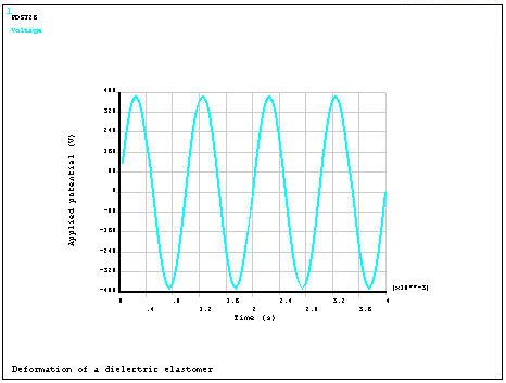
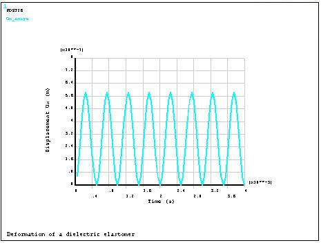
For a sinusoidal load, the longitudinal displacement as a function of time.
The elastomer has the following properties:
| Young's modulus (Y) = 3.6e6 Pa |
| Poisson's ratio (mu) = 0.4999 |
| Electric relative permittivity (eps) = 8.8 |
Free-space permittivity (eps0) is 8.854e-12 F/m.
The geometric properties are:
| Elastomer length (l) = 1.1 mm |
| Elastomer width (w) = 0.11 mm |
| Elastomer thickness (t) = 0.055 mm |
Loading conditions for this problem are:
| Electric field intensity (Ef0) = 7e6 V/m |
| Applied voltage (V) = Ef0*t Volts |
| Operating frequency (freq) = 1000 Hz |
The elastomer deformation is shown in the following animation:

The strain in the thickness direction is calculated to be -1.06e-3. That agrees with the analytical solution obtained using the following equation from I. Diaconu, D. Dorohoi ("Properties of Polyurethane Thin Films," Journal of Optoelectronics and Advanced Materials, Vol. 7, No. 2, pp. 921–924, April 2005).
S = -1/2 (ε0εr/Y) (E)2(1 + 2μ)
where ε0 is the free space permittivity, εr is the relative electrical permittivity, Y is Young's modulus, E is the applied electric field, and μ is the Poisson's ratio.
For the transient load, the elastomer response frequency is twice the frequency of the driving voltage due to the quadratic dependence of strain on the electric field.
/title, Deformation of a dielectric elastomer
/nopr
! Geometry
l=1.1e-3           ! beam length, m
w=0.11e-3          ! electrode width, m
t=0.055e-3         ! thickness, m

! Loading
Ef0=7e6            ! electric field intensity, V/m
V=Ef0*t            ! applied voltage, V
freq=1000          ! operating frequency, Hz

! Material properties
Y=3.6e6            ! Young modulus, Pa
mu=0.4999          ! Poisson ratio (nearly incompressible rubber)
eps=8.8            ! electrical permittivity, relative
eps0=8.854e-12     ! free-space permittivity, F/m

/VUP,1,z
/VIEW,1,1,1,1

/nopr
/PREP7
et,1,SOLID226,1001 ! 20-node brick coupled-field element
mp,EX,1,Y
mp,PRXY,1,mu
mp,PERX,1,eps

block,-l/2,l/2,-w/2,w/2,0,t
esize,t/2
vmesh,1

! Structural BC
nsel,s,loc,x,-l/2
d,all,ux,0
nsel,r,loc,y,-w/2
d,all,uy,0
nsel,r,loc,z,0
d,all,uz,0
nsel,all

! Electrical BC
nsel,s,loc,z,0
nsel,r,loc,x,-l/2,l/2
nsel,r,loc,y,-w/2,w/2
cp,1,volt,all
ng=ndnext(0)       ! ground node
nsel,all

nsel,s,loc,z,t
nsel,r,loc,x,-l/2,l/2
nsel,r,loc,y,-w/2,w/2
cp,2,volt,all
nl=ndnext(0)       ! load node
nsel,all

/SOLU
antype,static
cnvtol,f,1,1.e-6
d,ng,volt,0
d,nl,volt,V        ! apply voltage difference
solve
fini

/POST1
pldisp,1           ! display deformed/undeformed shape
andscl             ! animate deformed/undeformed shape
nsel,s,loc,x,l/2
nd=ndnext(0)       ! pick node for display
nsel,r,node,,nd
prnsol,epel        ! print strain
nsel,all
fini

/com  **************************************************************************
/com   Expected results:
epelz=-eps0*eps*Ef0**2*(1+2*mu)/(2*Y)
/com   epelz=%epelz%
/com
/com   Reference: I. Diaconu, D. Dorohoi "Properties of Polyurethane Thin Films"
/com              Journal of Optoelectronics and Advanced Materials, v.7, no.2,
/com              April 2005, pp. 921-924
/com  **************************************************************************

/PREP7
et,2,CIRCU94,4,1         ! voltage source, negative electric charge option
r,2,,V,freq
type,2
real,2
*get,nod226,node,,count  ! number of nodes
n,nod226+1
e,nl,ng,nod226+1

ddele,nl,volt
fini

/SOLU
antype,trans
time,4/freq
deltime,1/freq/20
outres,all,all
solve
fini

npost=node(l/2,0,0)      ! node for postprocessing

/POST26
nsol,2,nl,volt,,Voltage
nsol,3,npost,u,x,Ux_ansys
/axlab,x, Time (s)
/axlab,y, Applied potential (V)
plvar,2
/axlab,y, Displacement Ux (m)
plvar,3

/com  **************************************************************************
/com   Expected results:
/com   Ux=epelx*l
/com    where:
/com   - epelx=sigx/Y-mu/Y*sigy-mu/Y*sigz= sigMx/Y
/com   - stresses sigx=sigy=sigMx;   sigz=-sigMx
/com   - electric field Ef=Ef0*sin(om*t)
/com   - circular frequency om=2*pi*freq
/com   - Maxwell stress sigMx=eps0*eps*Ef**2/2
/com                         =eps0*eps*Ef0**2*(1-cos(2*om*t))/4
/com    therefore:
/com   Ux=eps0*eps*Ef0**2*l/(4*Y)*(1-cos(2*om*t))
/com  **************************************************************************

! Calculations for the analytical solution
pi=acos(-1)
om=2*pi*freq
epelx0=eps0*eps*Ef0**2*l/(4*Y)

*dim,work1,array,80
*dim,work2,array,80
filldata,4,,,,1
prod,5,1,,,,,,2*om
vget,work1(1),5
*vfun,work2(1),cos,work1(1)
vput,work2(1),6
add,7,4,6,,,,,,-1
prod,8,7,,,Ux_expec,,,epelx0

prvar,3,8
fini
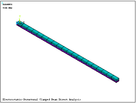
In this example problem, an electrostatic-structural analysis is performed to determine the deflection of a silicon beam for a MEMS switch.
The following topics are available:
A clamped silicon beam for a MEMS switch is suspended above an air gap. Forces generated by an electrostatic field bend the beam towards a ground plane. An electrostatic-structural analysis is performed to determine the center deflection versus applied voltage.
SOLID186 structural brick elements model the beam. SOLID226 "elastic air" (KEYOPT(4) = 1) elements of tetrahedral shape model the air below the beam. Midside nodes on the air elements are dropped to alleviate mesh distortion. Displacement constraints are imposed on the bottom surface and sides of the air mesh. The bottom surface of the air gap is grounded. A ramped voltage up to 178 volts is applied to the top air surface at 10 volt solution intervals. Large-deflection and stress-stiffening effects are enabled (NLGEOM,ON).
Geometric and material properties are input in the μMKSV system of units. For more information on units, see System of Units.
The geometric properties are:
| Beam length = 150 µm |
| Beam height = 2 µm |
| Beam width = 4 µm |
| Air gap = 2 µm |
The beam has the following material properties:
| Young's modulus = 169e3 MPa |
| Poisson's ratio = 0.066 |
| Density = 2.329e-15 kg/(µm)3 |
The "elastic air" is assigned the following material properties:
| Young's modulus = 1.0e-3 MPa |
| Poisson's ratio = 0.0 |
| Electric relative permittivity = 1.0 |
Free-space permittivity is 8.854e-6 pF/µm.
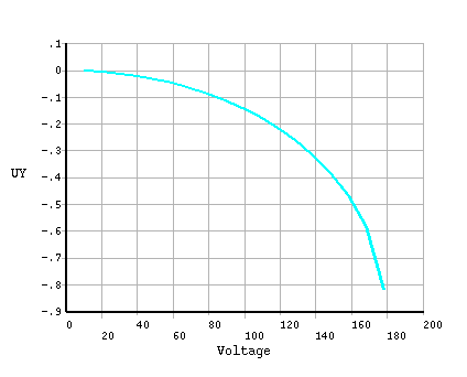
The mid-span deflection is shown as a function of applied voltage in the following figure. The maximum applied voltage of 178 volts produces a displacement of UY = -0.82 µm. Higher voltages produce beam snap-down and a diverging solution.
/title, Electrostatic-Structural Clamped Beam Direct Analysis
/nopr
! Problem parameters (uMKSV system)
l=150                    ! length of beam, um
tc=2                     ! beam height, um
w=4                      ! beam width, um
ta=2                     ! gap, um

V=178                    ! applied voltage, V
epse=1                   ! air permittivity, relative

/PREP7
et,1,SOLID186,,1         ! 20-node structural brick
mp,ex,1,169e3            ! MPa
mp,nuxy,1,0.066
mp,dens,1,2.329e-15      ! kg/(um)^3


et,2,SOLID226,1001,,,1   ! 20-node "elastic air" brick
mp,ex,2,1.e-3            ! MPa
mp,prxy,2,0.0
mp,perx,2,1
emunit,EPZRO,8.854e-6    ! pF/um

block,0,l,0,tc,,w
block,0,l,-ta,0,,w
vglue,all


vsel,s,volu,,1           ! mesh beam
aslv
lsla
lsel,r,loc,x,l/2
lesize,all,,,20,,,,1     ! 20 bricks along beam length
lsla
lsel,r,loc,y,tc/2
lesize,all,,,2,,,,1      ! 2 bricks along beam thickness
lsla
lsel,r,loc,z,w/2
lesize,all,,,1,,,,1      ! 1 brick along beam width
type,1
mat,1
vmesh,1


msha,1,3d                ! set element shape to tet
mshmid,2                 ! drop mid-side nodes
vsel,s,volu,,3           ! mesh air gap

aslv
lsla

lsel,r,loc,x,l/2
lesize,all,,,20,,,,1     ! 20 tets along air gap bottom
lsla
lsel,r,loc,y,-ta/2
lesize,all,,,1,,,,1      ! 1 tet along beam thickness

lsla
lsel,r,loc,z,w/2
lesize,all,,,1,,,,1      ! 1 tet along beam width
type,2
mat,2
vmesh,3

/view,1,1,1,1
/number,1
/pnum,type,1
eplot
fini


/SOLU
nsel,s,loc,x,0         ! structural BC
nsel,a,loc,x,l
d,all,ux,0
d,all,uy,0
d,all,uz,0
nsel,s,loc,y,-ta
d,all,ux,0
d,all,uy,0
d,all,uz,0
nsel,all

nsel,s,loc,y,-ta       ! electrical BC
d,all,volt,0           ! ground
nsel,s,loc,y,0
d,all,volt,V           ! electrode
nsel,all


cnvtol,f,1,1e-3
deltim,10              ! 10 Volt solution interval
outres,nsol,1
neqit,50
nlgeom,on
time,V                 ! Time = voltage
kbc,0                  ! ramped loading
solve
fini

ndisp=node(l/2,0,0)    ! node for displacement display

/POST26
nsol,2,ndisp,u,y
/axlab,y,UY
/axlab,x,Voltage
prvar,2
plvar,2
fini
The following example illustrates a comb drive electrostatic problem. One finger is modeled.
The following topics are available:
The air gap between a comb-drive rotor and a stator is meshed with PLANE223, KEYOPT(1) = 1001, elements. The electrodes are modeled as the coupled equipotential sets of nodes. The stator is fixed. The rotor is attached to the spring and allowed to move (Ux). Ground nodes are allowed to move horizontally. Equilibrium between the spring force and the electrostatic force is reached at: ux = 0.1 µm.
The reference solution is calculated based on the work of W. C. Tang et al ("Electrostatic-comb drive of lateral polysilicon resonators", Sensors and Actuators A:Physical, 21-23 (1990), 328-331). The target electrostatic force Fe can be calculated using:
Fe = (N)(h)(Eps0)(V)2/(g + ux)
where N is the number of fingers, h is the thickness in Z, Eps0 is the free space permittivity, V is the driving voltage, g is the initial lateral gap, and ux is the lateral displacement of the comb drive.
The potential distribution of the deformed comb drive is shown in Figure 2.31: Potential Distribution on Deformed Comb Drive.
The command listing below demonstrates the problem input. Text prefaced by an exclamation point (!) is a comment.
/batch,list
/com
!-------------- Combdrive Parameters ---------------------

eps0=8.854e-6                ! Free space permittivity
g0=5.0                       ! Initial gap
h=10                         ! Fingers width (in-plane)
L=100                        ! Finger length
x0=0.5*L                     ! Fingers overlap
esize=0.5                    ! Element size
k=2.8333e-4                  ! Spring stiffness
vltg=4.0                     ! Applied voltage

!-------------- Combdrive Finger Geometry ---------------

/prep7
et,1,223,1001,,,1            ! "Elastic air" option
emunit,epzro,eps0
mp,perx,1,1
mp,ex,1,1e-7
mp,nuxy,1,0.0

et,2,14,,1                   ! Linear spring, UX degree of freedom
r,2,k                        ! Spring parameters (k/2)

et,3,183                     ! PLANE183 for moving finger
mp,ex,2,169e3
mp,nuxy,2,0.25

BLC4,0,-h/2,L,h              ! Create all areas
BLC4,-h,-h/2,h,h
BLC4,-h,-h-g0,h,h/2+g0
BLC4,-h,h/2,h,h/2+g0
BLC4,L-x0,h/2+g0,L,h/2
BLC4,L-x0,-h-g0,L,h/2
BLC4,0,-h-g0,2*L-x0,2*(h+g0)

aovlap,all
nummrg,kp

! --------------------- Areas Attributes --------------------

asel,s,area,,1               ! Moving finger
asel,a,area,,8
asel,a,area,,9
asel,a,area,,10
aatt,2,3,3                   ! Material 2, real 3, type 3

asel,s,area,,11              ! Air gap
aatt,1,1,1                   ! Material 1, real 1, type 1
alls

!-------------------- Air Gap Free meshing ------------------

asel,s,area,,11
esize,esize
mshkey,0
amesh,all
alls

!-------------------- Meshing of Moving finger  ------------------

asel,s,area,,1
asel,a,area,,8
asel,a,area,,9
asel,a,area,,10

esize,esize
mshape,0,2
mshkey,1
amesh,all
alls

!------------------- Spring Element -----------------

type,2
real,2

*get,node_num,node,,count
n,node_num+1,0.0,0.0
nsel,s,loc,x,-h
nsel,r,loc,y,0.0
*get,node0,node,,num,max
e,node0,node_num+1
alls

! ------------- Nodal components for BC ---------------

LSEL,s,line,,15
LSEL,a,line,,33
LSEL,a,line,,3
LSEL,a,line,,2
LSEL,a,line,,1
LSEL,a,line,,31
LSEL,a,line,,9

NSLL,S,1
cm,rotor,node                ! Component 'rotor'
alls

LSEL,s,line,,20
LSEL,a,line,,17
LSEL,a,line,,37
LSEL,a,line,,23
LSEL,a,line,,24

NSLL,S,1
cm,ground,node               ! Component 'ground'
alls

fini

!------------- Boundary conditions -----------
/solu

nsel,s,loc,y,-(h+g0)         ! Symmetry (uy=0)
nsel,a,loc,y,h+g0
d,all,uy,0
alls

d,node_num+1,ux,0.0          ! Fix the spring (ux=0)

cmsel,s,ground               ! Ground (ux=uy=volt=0)
d,all,volt,0.0
d,all,uy,0.0
alls

LSEL,s,line,,20              ! Fix horizontal (ux=0)
LSEL,a,line,,37
LSEL,a,line,,24
NSLL,S,1

d,all,ux,0.0

cmsel,s,rotor                 ! Apply voltage to rotor
d,all,volt,vltg
alls

fini

!---------------- Solution ----------------------------

/solu
nlgeom,on
outres,all,all
cnvtol,f,1,1e-5
solve
fini

!---------------- Postprocessing ---------------------

/post1
/out
set,last,last
*get,ux_1,node,node0,u,x

CMSEL,s,ground
/com --------------------------------------------
/com Components of electrostatic force on stator:
/com --------------------------------------------
emft

Fe=-eps0*vltg**2/(g0+ux_1)
/com,
/com, *** Expected force Fe = %Fe%
/com
/com
/com Displacement of the combdrive (Ux):
*vwrite,ux_1
(/' Combdrive displacement = ',e13.6)
ux_ref=0.1
*vwrite,ux_ref
(/' Reference displacement = ',e13.6)

fini
This example problem is an electrostatic-structural analysis to determine the deformation of a folded dielectric elastomer actuator (described in F. Carpi, C. Salaris and D. De Rossi, “Folded Dielectric Elastomer Actuators,” Smart Materials and Structures, v16, 300-305 (2007)).
The following topics are available:
The actuator is fabricated by coating the surfaces of a thin dielectric elastomer with compliant electrodes, then folding it into many layers to produce a multi-layer stack of capacitors. The elastomer contracts when a high voltage is applied between the electrodes. The electrostatic force compresses the elastomer thickness and increases its area due to lateral expansion produced by the Poisson effect.
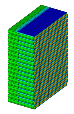
SOLID225 elements with structural and electric degrees of freedom (KEYOPT(1) = 1001) coupled by the electrostatic force are used to discretize a half-symmetry model of the actuator, as shown:
Fixed displacements constraints are imposed on the bottom surface of the actuator. A voltage of 10625 V is applied to the top electrode; the bottom electrode is grounded.
The geometric properties are:
| Actuator height = 34 mm |
| Actuator width = 25 mm |
| Electrode width = 15 mm |
The elastic behavior of the silicon rubber material forming the elastomer under compression was approximated by Yeoh’s hyperelastic model. The axial stress-strain curve reported in F. Carpi et al. was curve-fit to a 3rd order (N = 3) Yeoh strain energy density function with the following constants:
| C10 = 6742.40080183932 MPa |
| C20 = -301.48251973889 MPa |
| C30 = 186.326705722713 MPa |
| d1 = d2 = d3 = 0 |
The electric behavior was characterized by relative linear permittivity:
| Electric relative permittivity = 4.5 |
A static voltage load is applied in 17 steps to obtain a coupled-field solution. Large-deflection and stress-stiffening effects are enabled (NLGEOM,ON). The nonlinear solution convergence is based on displacement, force and electric charge equilibrium, as well as volume conservation. The volume conservation needed to characterize the fully incompressible silicon elastomer is ensured by an automatic activation of the mixed u-P formulation (KEYOPT(11) = 1) with SOLID225.
Total axial strain was calculated as the maximum displacement of the top surface divided by the actuator length times 100 (%):
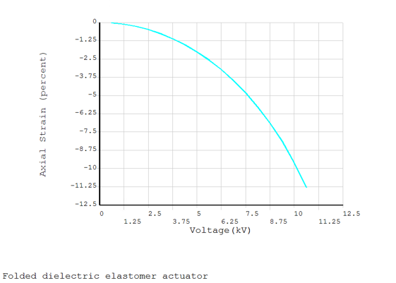
The strain vs. voltage curve shows that compressive instability is approaching and will occur at voltages not much higher than the ones used.
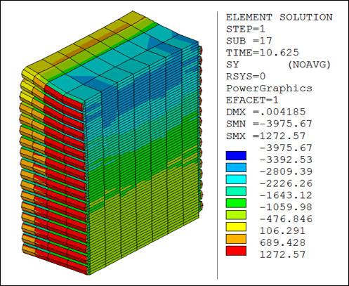
The following figure shows the corresponding axial stress distribution:
Following is the problem input. All text prefaced with an exclamation point (!) is a comment.
/title, Folded dielectric elastomer actuator
/nopr
W=25             ! width, mm
D=13             ! depth, mm
thk=1            ! layer thickness, mm
nfolds=17        ! number of times the elastomer is folded
nlayers=2*nfolds ! number of layers
L=thk*nlayers    ! length, mm
W_elec=15        ! electrode width, mm
fscale=1e-3      ! scale factor (mm to m)

perx_val=4.5     ! relative permittivity

E=10.625         ! applied electric field, V/um
V=E*thk/fscale   ! voltage, V

/prep7
! Solid model
*do,_layer,1,nlayers
 rect,,W,thk*(_layer-1),thk*_layer
*enddo

*do,_i,1,nlayers/2
 wpoff,W,thk
 pcirc,thk,,-90,0
 pcirc,thk,,0,90
 *if,_i,ne,nlayers/2,then
  wpoff,-W,thk
  pcirc,thk,,90,180
  pcirc,thk,,180,270
 *endif
*enddo
nummrg,kp

vext,all,,,,,W_elec/2    ! z=0 is symmetry plane

asel,s,loc,z,W_elec/2
vext,all,,,,,W/2-W_elec/2
nummrg,kp

! Element type
et,1,225,1001            ! electrostatic-structural analysis

! Material models
mp,perx,1,perx_val

tb,hyper,1,1,3,yeoh
tbdata,1,6742.40080183932,-301.48251973889,186.326705722713,0,0,0

! Meshing
esize,4*thk
vmesh,all

! Electrical boundary conditions
*do,_yval,0,nlayers,2
 nsel,s,loc,y,_yval-.1,_yval+.1
 nsel,r,loc,x,0,W
 nsel,r,loc,z,0,W_elec/2
 d,all,volt,0
*enddo

*do,_yval,1,nlayers,2
nsel,s,loc,y,_yval-.1,_yval+.1
nsel,r,loc,x,0,W
nsel,r,loc,z,0,W_elec/2
d,all,volt,V
*enddo
nsel,all

! Frictionless base structural constraint
nsel,s,loc,y,0
d,all,uy,0
nsel,r,loc,x,0
d,all,ux,0
nsel,r,loc,z,0
d,all,uz,0
nsel,all

! Symmetry Plane
nsel,s,loc,z,0
d,all,uz,0
nsel,all

vlscale,all,,,fscale,fscale,fscale,,,1
finish

/solu
antyp,static
kbc,0
nlgeom,on
nsub,17
autots,off
outres,all,1
time,E           ! E in V/um
solve
finish

/post1
set,last
plns,s,y
*get,uy_min,plnsol,,min
uy_max=abs(uy_min)
overall_strain=-100*uy_max/(L*fscale)   ! %

/post26
n_top=node(W/2,nlayers*thk,0) !
nsol,2,n_top,uy
prod,3,2,,, ,,,100/(L*fscale)   ! strain, %
/axlab,x,Voltage(kV)
/axlab,y,Axial Strain (percent)
plvar,3
finish
This example demonstrates a nonlinear static analysis and a linear perturbation modal analysis of a miniature clamped-clamped beam.
The following topics are available:
Miniature clamped-clamped beams with dimensions in the micrometer range are widely used in MEMS. Typical applications are resonators for RF filters, voltage controlled micro switches, adjustable optical gratings, or test structures for material parameter extraction. Clamped-clamped beams can behave in a highly nonlinear fashion due to deflection-dependent stiffening and stiffening caused by prestress. Both effects are very important for MEMS analysis and are illustrated by this example.
The example demonstrates:
a nonlinear static analysis to determine the beam deflection up to the pull-in voltage;
a linear perturbation modal analysis of the beam subject to a DC voltage bias.
Both analyses consider:
a beam without structural preload;
a beam with initial structural prestress modeled via thermal expansion.
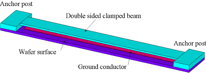
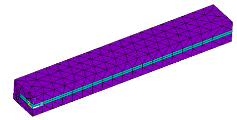
The half symmetry model uses hexahedral solid elements (SOLID185) for the structural domain and tetrahedral elements (SOLID226) with the elastic air option (KEYOPT(4) = 1) for the electrostatic domain. The elastic air elements have both structural (UX, UY, UZ) and electrostatic (VOLT) degrees of freedom. The beam is fixed on both ends, and symmetry boundary conditions are applied on the plane of intersection. The outer boundary of the elastic air domain is also fixed.
The analysis input and corresponding results are presented in the following sections:
Model Input
/TITLE, Clamped-clamped beam with fringe field
! µMKSV system of units

! Model parameters

B_L=100                  ! Beam length
B_W=20                   ! Beam width
B_T=2                    ! Beam thickness
F_L=4                    ! Farfield in beam direction
F_Q=4                    ! Farfield in cross direction
F_O=4                    ! Farfield above beam
E_G=4                    ! Electrode gap

/VIEW,1,1,-1,1
/PNUM,TYPE,1
/NUMBER,1
/PBC,ALL,1
/PREP7
ET,1,SOLID185,,3         ! Simplified enhanced strain
ET,2,SOLID226,1001       ! Electrostatic-structural analysis
KEYOPT,2,4,1              ! Elastic air

MP,EX,1,169e3            ! Material properties Si
MP,NUXY,1,0.066          ! <110>
MP,DENS,1,2.329e-15
MP,ALPX,1,1e-6

EMUNIT,EPZRO,8.85e-6     ! Free space permittivity
MP,PERX,2,1              ! Relative permittivity of air
MP,EX,2,1e-6
MP,PRXY,2,0

! Half symmetry

BLOCK,0,B_L,0,B_W/2+F_Q,-E_G,B_T+F_O    ! Entire domain
BLOCK,0,B_L,0,B_W/2,0,B_T               ! Structural domain
BLOCK,0,B_L,0,B_W/2,-E_G,0
VOVLAP,ALL

LSEL,S,LOC,X,B_L/2       ! Mesh density in axial direction
LESIZE,ALL,,,20,,1
LSEL,S,LOC,Y,B_W/4       ! Mesh density in transverse direction
LESIZE,ALL,,,2,,1
LSEL,S,LOC,Z,B_T/2       ! Mesh density in vertical direction
LESIZE,ALL,,,2,,1
LSEL,ALL
VSEL,S,LOC,Z,B_T/2       ! Mesh structural domain (mapped meshing)
VMESH,ALL
VSEL,ALL

SMRTSIZ,2
MSHAPE,1,3D
MSHKEY,0
TYPE,2
MAT,2
VMESH,4

LSEL,S,LOC,Y,B_W/2+F_Q   ! Mesh density at bottom electrode
LSEL,R,LOC,X,B_L/2
LESIZE,ALL,,,19,,1
LSEL,S,LOC,Y,0           ! Mesh density at bottom electrode
LSEL,R,LOC,Z,B_T+F_O
LESIZE,ALL,,,19,,1
LSEL,S,LOC,Y,(B_W+F_Q)/2
LESIZE,ALL,,,4,1/5,1
LSEL,ALL
VMESH,ALL

VSEL,S,LOC,Z,B_T/2       ! Movable electrode
ASLV,S,1
ASEL,U,LOC,Y,0
ASEL,U,LOC,X,0
ASEL,U,LOC,X,B_L
NSLA,S,1
CP,1,VOLT,ALL
NLOAD=NDNEXT(0)
ALLSEL

ASEL,S,LOC,Z,-E_G        ! Fixed ground electrode
NSLA,S,1
CP,2,VOLT,ALL
NGROUND=NDNEXT(0)
ALLSEL

ASEL,S,LOC,Z,B_T/2
ASEL,R,LOC,Y,B_W/4
NSLA,S,1
CM,FIXA,AREA             ! Boundary condition must be
DA,ALL,UX                ! applied on solid model entities
DA,ALL,UY
DA,ALL,UZ

ASEL,S,LOC,Z,B_T/2
ASEL,R,LOC,Y,0
NSLA,S,1
CM,BCYA,AREA
DA,ALL,UY
ALLSEL

NSEL,S,LOC,Z,-E_G         ! Fix outer boundary of the air domain
NSEL,A,LOC,Z,B_T+F_O
NSEL,A,LOC,Y,B_W/2+F_Q
D,ALL,UX,0
D,ALL,UY,0
D,ALL,UZ,0
ALLSEL

FINI
Calculation of the Beam Displacement Up to Pull-in
Two nonlinear static analyses (of an unloaded and of a prestressed beam) are performed up to the respective pull-in voltages to determine the beam deformation.
The pull-in voltage for each case has been determined in advance as the highest voltage load that produces a converged solution.
Beam without initial prestress: 1284 V
Beam with initial prestress: 1414 V
Geometric nonlinearities are enabled (NLGEOM,ON) to capture the effect of stress-stiffening of the beam and the counteractive effect of electrostatic softening produced by the electric force.
V1=1284                   ! Pull-in voltage (no prestress)

/solu
antype,static
outres,all,all

d,nload,volt,V1
d,nground,volt,0

kbc,0
nsubst,15
nlgeom,on
time,V1
solve
fini

n1=node(b_l/2,0,0)       ! Define master nodes
n2=node(b_l/4,0,0)

/post26
*dim,_uz1,table,20
*do,_i,1,20
_uz1(_i)=-e_g
*enddo

nsol,2,nload,volt,,VOLT
nsol,3,n1,u,z,UZ
nsol,4,n2,u,z,UZ
prvar,2,3,4
vget,_uz1,3

rfor,5,nload,chrg,,CHRG ! Negative charge
prod,6,5,,,CAP,,,-1/V1
prvar,6
/xrange,0,V1
/axlab,x,Voltage
/axlab,y, Capacitance
plvar,6
fini
The following figure shows the increase of capacitance between the ground plane and the beam electrode as the air gap decreases with beam deflection.

The initial biaxial prestress of 100 kPa is modeled via thermal expansion in order to realize a nonuniform stress distribution at the clamp.
V2=1414                   ! Pull in voltage for the beam with initial prestress

/solu
antype,static
outres,all,all

kbc,0
nlgeom,on

tref,0
sigm_b=-100
tunif,sigm_b*(1-0.066)/(169e3*1e-6) ! Thermal prestress

nsubst,15
time,V1
d,nload,volt,V1
solve

nsubst,5
time,V2
d,nload,volt,V2
solve

fini

/post26
nsol,2,nload,volt,,VOLT
nsol,3,n1,u,z,UZ_PRES
nsol,4,n2,u,z,UZ
prvar,2,3,4
/axlab,x,Voltage
/xrange,0,V2
/axlab,y,UZ
/yrange,-3,0
vput,_uz1,5,,,UZ
plvar,3,5
fini
The following figure compares the mid-span deflection of an unloaded (UZ) and prestressed (UZ_PRES) beam.

The following figure shows the distribution of the electric field density (EF) in the air domain. Notice an almost uniform field in the air gap below the beam and the fringing field around the beam edge.

Calculation of Resonance Frequency of the Beam with DC-voltage Bias
The following command input illustrates the modal analysis of a beam with a DC-voltage bias. The input corresponds to the previous case of a structure with initial prestress. Set TUNIF to zero in this file if initial prestress is not considered.
First, a nonlinear static analysis is performed with a voltage load V = 1000 V. It is followed by a linear perturbation modal analysis using the Block Lanczos solver (MODOPT,LANB) to determine the first five eigenmodes of the beam with both the initial prestress and the DC-voltage bias. Setting the driving electrode voltage to zero (short-circuit condition) in the linear perturbation modal analysis produces the resonance frequency of the beam.
/com, Apply DC voltage V to a beam with initial prestress
V=1000                   ! Bias voltage

/solu
antype,static
outres,all,all

d,nload,volt,V           ! Apply bias voltage

kbc,0
nsubst,1
nlgeom,on
solve
fini

parsave

/com,
/com,  LP Modal analysis (resonance)
/com,
/solu
antype,static,restart,last,last,perturb
perturb,modal
solve,elform

parresu
d,nload,volt,0           ! Resonance frequency BC

modopt,lanb,5
mxpand                   ! Expand all modes
solve
fini

/post1
file,,rstp
set,1,1
pldisp
fini

Calculation of the Anti-resonance Frequency of the Beam with DC-voltage Bias
Leaving the driving electrode voltage free (open-circuit condition) in the linear perturbation modal analysis produces the anti-resonance frequency of the beam.
/solu
antype,static,restart,last,last,perturb
perturb,modal
solve,elform

ddele,nload,volt    ! Anti-resonance frequency BC

modopt,lanb,5
mxpand              ! Expand all modes
solve
fini
The following table compares the purely structural resonance frequency of the beam with the resonance and anti-resonance frequencies of the beam with the DC-voltage (1000 V) bias.
Table 2.20: Resonance Frequencies of the Fundamental Mode
| Fundamental Frequency, Hz | Structural | Electrostatic-Structural | |
|---|---|---|---|
| Resonance | Anti-Resonance | ||
| Without initial prestress | 1763643.5 | 1724286.2 | 2037445.2 |
| With initial prestress | 2086978.2 | 1932764.9 | 2161037.7 |
This example demonstrates a nonlinear static analysis, a linear perturbation harmonic analysis, and a nonlinear transient analysis of a micromirror cell.
The following topics are available:
The micromirror cell is part of a complex mirror array used for light deflection applications. The entire mirror array consists of six separate mirror strips driven synchronously in order to achieve high-speed light deflection. Each strip is attached to the wafer surface by two intermediate anchor posts. Due to the geometrical symmetry, the mirror strips can be divided into three parts whereby just one section is necessary for finite element analysis.
The example demonstrates:
a nonlinear static analysis to determine the mirror deflection up to the pull-in voltage;
a linear perturbation harmonic analysis of the mirror subject to a DC voltage bias;
a nonlinear transient analysis to determine the mirror deflection in response to a sawtooth voltage load.
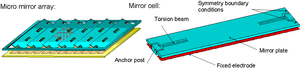
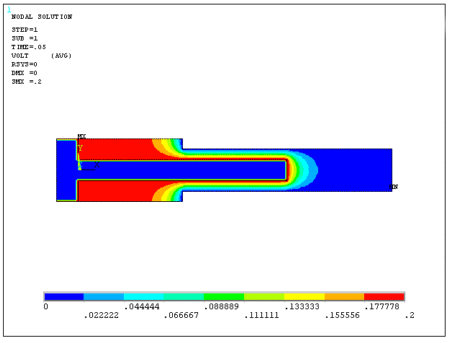
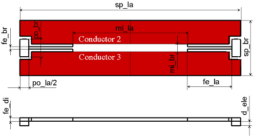
The electrostatic domain consists of three conductors. The nodes of the mirror itself are defined by node component COND1, and the fixed ground conductors are node components COND2 and COND3. The fixed conductors are on top of the ground plate shown in Figure 2.41: Schematic View of a Micro Mirror Array and a Single Mirror Cell and Figure 2.42: Parameter Set for Geometrical Dimensions of the Mirror Cell.
The model uses hexahedral solid elements (SOLID185) for the structural domain and tetrahedral elements (SOLID226) with the elastic air option (KEYOPT(4) = 1) for the electrostatic domain. The elastic air elements have both structural (UX, UY, UZ) and electrostatic (VOLT) degrees of freedom to account for the deformation of the air domain under the mirror plate.
The analysis input and corresponding results are presented in the following sections:
| Model Input |
| Calculation of Voltage Displacement Up to Pull-in |
| Linear Perturbation Harmonic Analysis with a Polarization Voltage |
| Nonlinear Transient Analysis |
Model Input
/TITLE, Silicon micromirror cell
/PREP7
                                 ! uMKSV units
fe_la=200                        ! Spring length
fe_br=10                         ! Spring width
fe_di=15                         ! Spring thickness
sp_la=1000                       ! Mirror length
sp_br=250                        ! Mirror width
mi_la=520                        ! Length center part
mi_br=35                         ! Width center part
po_la=80                         ! Length of anchor post
po_br=80                         ! Width of anchor post
fr_br=30                         ! Fringing field distance
d_ele=20                         ! Electrode gap

ET,1,SOLID185,,3                 ! Structural domain
MP,EX,1,169e3                    ! Material properties of Si
MP,NUXY,1,0.066
MP,DENS,1,2.329e-15
MP,DMPS,1,0.05                   ! Damping

ET,2,SOLID226,1001               ! Electrostatic domain
KEYOPT,2,4,1                     ! Elastic air

EMUNIT,EPZRO,8.85e-6             ! Free space permittivity
MP,PERX,2,1                      ! Relative permittivity of air
MP,EX,2,0.00000005               ! MPa
MP,PRXY,2,0.0

del1=(mi_br-fe_br)/2

K,1
K,2,,fe_br/2
K,3,,mi_br/2
K,4,,po_br/2+(mi_br-fe_br)/2
K,5,,sp_br/2
K,6,,sp_br/2+fr_br

KGEN,2,1,6,1,mi_la/2
KGEN,2,1,6,1,mi_la/2+fe_la-(mi_br-fe_br)/2
KGEN,2,1,6,1,sp_la/2

K,21,sp_la/2,po_br/2
K,13,sp_la/2-po_la/2
K,14,sp_la/2-po_la/2,fe_br/2
K,25,sp_la/2-po_la/2,po_br/2

A,3,9,10,4
A,9,15,16,10
A,4,10,11,5
A,10,16,17,11
A,16,22,23,17

AGEN,2,ALL,,,,,-d_ele
ASEL,S,LOC,Z,-d_ele
AADD,ALL
ASEL,ALL

A,1,7,8,2
A,2,8,9,3
A,7,13,14,8
A,13,19,20,14
A,14,20,21,25

ASEL,S,LOC,Z,0
VEXT,ALL,,,,,fe_di
ASEL,ALL
ASEL,S,AREA,,9,10
VEXT,ALL,,,,,-d_ele
ASEL,ALL
VATT,1,,1

BLOCK,0,sp_la/2,o,sp_br/2+fr_br,-d_ele,fe_di

VDELE,13
AOVLAP,ALL

ASEL,S,LOC,Z,fe_di
ASEL,A,LOC,Z,-d_ele
ASEL,A,LOC,X,0
ASEL,A,LOC,X,sp_la/2
ASEL,A,LOC,Y,0
ASEL,A,LOC,Y,sp_br/2+fr_br

VA,ALL

VSBV,13,ALL,,,KEEP

VSEL,S,VOLU,,14
VATT,2,,2
VSEL,ALL

ESIZE,,2                            ! Mesh density parameter
LESIZE,68,,,1,,1                    ! Spring width (quarter model)
LESIZE,77,,,10,,1                   ! Spring length
LESIZE,67,,,5,,1                    ! Length center part
LESIZE,82,,,2,,1                    ! Anchor post
LESIZE,51,,,5,,1
LESIZE,62,,,2,,1
                                    ! Y-direction
LESIZE,87,,,2,,1                    ! Anchor post
LESIZE,75,,,1,,1                    ! Center part
LESIZE,42,,,1,,1                    ! Mirror center
LESIZE,54,,,3,,1                    ! Mirror outside part

VMESH,1,12

TYPE,2
MAT,2
SMRTSIZ,2
MSHAPE,1,3D
MSHKEY,0
ESIZE,,1
VMESH,14
ALLSEL

VSYM,X,ALL
VSYM,Y,ALL
NUMMRG,NODE,1e-5
NUMMRG,KP,1e-3

VSEL,S,TYPE,,1
ASEL,S,EXT
ASEL,U,LOC,X,sp_la/2
ASEL,U,LOC,X,-sp_la/2
ASEL,U,LOC,Z,fe_di
ASEL,U,LOC,Z,-d_ele
NSLA,S,1
CM,COND1,NODE
CP,1,VOLT,ALL
cn1=ndnext(0)
ALLSEL

ASEL,S,AREA,,11
ASEL,A,AREA,,128
NSLA,S,1
CM,COND2,NODE
CP,2,VOLT,ALL
cn2=ndnext(0)
ALLSEL

ASEL,S,AREA,,202
ASEL,A,AREA,,264
NSLA,S,1
CM,COND3,NODE
CP,3,VOLT,ALL
cn3=ndnext(0)
ALLSEL

VSEL,S,TYPE,,1
ASLV,S,1
ASEL,R,LOC,Z,-d_ele
NSLA,S,1
CM,FIXA,AREA                       ! Boundary condition must be
DA,ALL,UX                          ! applied on solid model entities
DA,ALL,UY                          ! Fixed boundary condition
DA,ALL,UZ
ALLSEL

ASEL,S,LOC,Z,-d_ele                ! Fix bottom electrodes
DA,ALL,UX
DA,ALL,UY
DA,ALL,UZ
ALLSEL

ASLV,S,1
ASEL,R,LOC,X,sp_la/2               ! Symmetry boundary conditions
DA,ALL,UX
NSLA,S,1

ASLV,S,1
ASEL,R,LOC,X,-sp_la/2
DA,ALL,UX
ALLSEL,ALL

mn1=node(0.0000,125.00,7.5000)   ! Node on the upper edge
mn2=node(0.0000,0.0000,7.5000)   ! Node at plate center
mn3=node(169.00,-104.29,0.0000)  ! Node at the lower edge

PARSAVE
Calculation of Voltage Displacement Up to Pull-in
This input demonstrates a nonlinear static analysis up to the pull-in voltage of 876 V.
/com, *** Nonlinear Static Analysis: pull-in

Vpi=876                          ! Pull-in voltage

/solu
antype,static
nlgeom,on
outres,all,all

d,cn1,volt,0
d,cn2,volt,Vpi
d,cn3,volt,0

autots,off
nsub,10
neqit,50
kbc,0
outres,all,1
time,Vpi
solve
fini

/post26
/axlab,x,Voltage
/axlab,y,Nodal displacements
nsol,3,mn1,u,z,up_edge            ! Node on the upper edge
nsol,4,mn2,u,z,center_n           ! Node at plate center
nsol,5,mn3,u,z,lo_edge            ! Node at the lower edge
prvar,3,4,5
plvar,3,4,5
fini
The displacement of the mirror upper edge, center, and lower edge are shown in the following figure:

Linear Perturbation Modal and Harmonic Analyses with a Polarization Voltage
The following example demonstrates the shift in the eigenfrequencies and the change of harmonic transfer functions at high polarization voltages of opposite signs, +800 V and -800 V, applied to fixed electrodes COND2 and COND3, respectively. Increasing the applied polarization voltage reduces the eigenfrequencies and shifts the resonance peak of the harmonic sweep to the left.
/com, *** Nonlinear Static Analysis with a DC-voltage load
/solu
antype,static
nlgeom,on
outres,all,all

d,cn1,volt,0
d,cn2,volt,800
d,cn3,volt,-800

autots,off
nsub,10
kbc,0
outres,all,1
solve
fini

/com, *** Linear Perturbation Modal Analysis with a DC-voltage load
/solu
antype,static,restart,last,last,perturb
perturb,modal
solve,elform
parresu

modopt,damp,10
mxpand,10
solve
*get,f1,mode,1,dfrq        ! damped frequency of mode 1
fini

/post1
/view,1,1,1,1
/vup,,z

file,,rstp
esel,s,enam,,SOLID185
nsle
set,,1
plnsol,u,z
set,,5
plnsol,u,z
alls
fini

/com, *** Linear Perturbation Harmonic Analysis
/solu
antype,static,restart,last,last,perturb
perturb,harm
solve,elform

parresu
harfrq,0,5e4
nsubst,70
kbc,1
d,cn1,volt,1
d,cn2,volt,0
d,cn3,volt,0
solve
fini

/post26
file,,rstp
/axlab,x,Frequency
/axlab,y,Nodal amplitude
nsol,3,mn1,uz,,up_edge
nsol,4,mn3,uz,,lo_edge
plvar,3,4
/axlab,y,Phase angle
plcplx,1
plvar,3,4

prcplx,1
prvar,3,4
fini
The shapes of the tilting and bending modes are shown in the following figures.


Harmonic transfer function amplitude and phase angle for the 800 V polarization voltage are shown in the following figures.


Nonlinear Transient Analysis
This input demonstrates the response of a sawtooth-like voltage function. The voltage displacement relationship is linearized since a high polarization voltage of 400 V is applied to both fixed electrodes. In practice, most mirror cells operate in a closed loop to a controller circuit to obtain better performance.
/com, *** Nonlinear Transient Analysis
cycle_t=500e-6             ! Cycle time of one saw tooth
                           ! about 20 times the cycle time of mode 1
rise_t=cycle_t/10          ! Rise time
num_cyc=3                  ! Number of cycles

/solu
antype,transient
nlgeom,on
deltime,rise_t/10,rise_t/10,rise_t/10
auto,off
outres,all,all

tintp,,0.25,0.5,0.5
trnopt,full,,,,,,,f1

kbc,0
j=1
*do,i,1,num_cyc
 time,cycle_t*(i-0.5)+rise_t*(i-1)
 d,cn1,volt,100
 d,cn2,volt,400
 d,cn3,volt,-400
 lswrite,j
 j=j+1
 time,cycle_t*(i-0.5)+rise_t*i
 d,cn1,volt,-100
 d,cn2,volt,400
 d,cn3,volt,-400
 lswrite,j
 j=j+1
*enddo

time,cycle_t*num_cyc+rise_t*num_cyc
d,cn1,volt,0
lswrite,j

lssolve,1,j
fini

/post26
nsol,4,mn1,u,z,up_edge            ! Node on the upper edge
nsol,5,mn2,u,z,center_n           ! Node at plate center
nsol,6,mn3,u,z,lo_edge            ! Node at the lower edge
prvar,4,5,6
/axlab,y, Upper Edge Displacement
plvar,4
/axlab,y, Plate Center Displacement
plvar,5
/axlab,y, Lower Edge Displacement
plvar,6
fini
The displacement of the mirror upper edge, center, and lower edge in response to the sawtooth voltage application are shown in the following figures.


