


The following modeling work is necessary for this example problem:
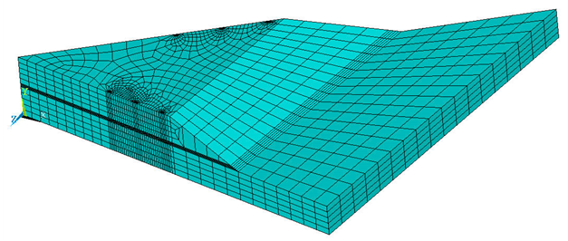
The completed model contains 57,134 nodes and 11,558 3D 20-node hexahedron structural solid elements.
Thermal element SOLID90 is used for all parts of the flip chip model as shown in this figure:
Temperature profiles at different time steps, obtained from transient thermal analysis, are used in nonlinear structural analysis to predict residual creep strains in solder bumps. The analysis requires the same mesh used for thermal analysis. It is therefore necessary to convert thermal element SOLID90 to structural element SOLID186 (ETCHG).
Contact and target elements CONTA174 and TARGE170, respectively, are compatible with structural element SOLID186, so those elements are not changed. Contact element options can be modified if necessary (KEYOPT).
The following input converts the element types:
ETCHG,TTS      ! Change thermal elements to structural elements
KEYOPT,3,1,0   ! Change degrees of freedom for TEMP to UX, UY and UZ
KEYOPT,3,2,2   ! Multipoint constraint
KEYOPT,3,9,1   ! Exclude both initial geometrical penetration or gap and offset
KEYOPT,3,12,5  ! Bonded contact
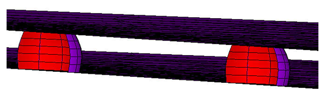
Surface-to-surface contact pairs are created between flip chip parts using CONTA174 and TARGE170 elements, as shown in this figure:
The following input creates a contact pair:
/COM, CONTACT PAIR CREATION - START
ET,2,170				! Define TARGET170 element
ET,3,174				! Define CONTACT174 element
KEYOPT,3,1,2		! Select temperature degree of freedom for thermal analysis
REAL,2					! Set the element real constant
RMODIF,2,14, 319.186992		! Define Thermal Contact Conductance (TCC)

! Generate the target surface
CMSEL,S,CHIP_DOWN.TGT,NODE	! Selected user-defined nodal component for target.
TYPE,2					! Element type for target elements
ESLN,S,0				! Select elements attached to nodal component
ESURF					! Generate target mesh on the free faces of selected elements.
ALLSEL,ALL

! Generate the contact surface
CMSEL,S,SOLDER_TOP.CNT	! Selected user-defined nodal component for contact.
TYPE,3					! Element type for contact elements
ESLN,S,0				! Select elements attached to nodal component
ESURF					! Generate contact mesh on the free faces of selected elements.
ALLSEL
/COM, CONTACT PAIR CREATION - END
Similarly, contact pairs are created between other parts of the flip chip.