


The flip chip package is composed of the chip, underfill, substrate, and solder as shown in the following figures:
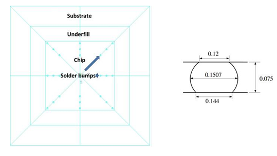
The size of the chip is 6.95 mm × 6.95 mm ×0.6 mm. The size of the substrate is 14 mm ×14 mm × 0.65 mm. The distance between chip and substrate is 0.075 mm. The diameter of the upper pad, the diameter of the lower pad, and the width of the solder bump are 0.12 mm, 0.144 mm, and 0.1507 mm, respectively.
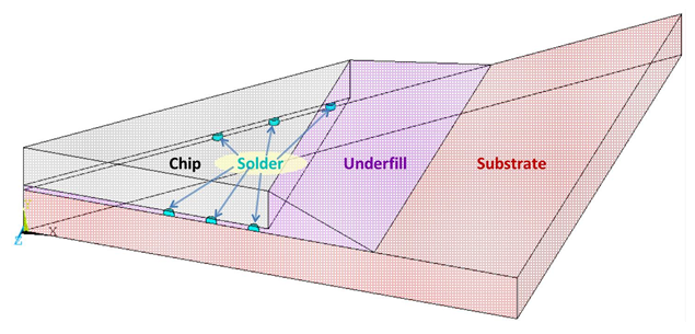
To minimize the number of degrees of freedom, and therefore the computational resources required for the thermomechanical analysis, a 1/8 symmetry of the full model is used. To determine the cyclic thermal load effect on the solder joint, a generalized Garofalo creep model is used for the secondary stage of the creep analysis.