CPA RLGC Simulation Setup
Follow these steps to set up the options for a CPA simulation.
If the design model contains one or more solderballs, each solderball's height must be greater than 5um (i.e., approx 0.196850 mils). Refer to Adding Solderballs to a Package.
- Navigate to the Simulation tab.
- From the CPA area, click Options to open the CPA Options window.
-
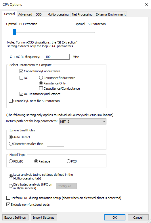
Use the slider to set the Refinement to either of the following:
- Optimal - PI Extraction - provides a balanced trade-off between simulation performance and accuracy.
- Optimal - SI Extraction - provides a final, exhaustive analysis. This option uses the most amount of computer memory and CPU time. When this option is selected, loop-based RLCG data is extracted. However, if the Q3D option is selected, only partial RLCG is extracted.
-
Enter a value greater than zero in the G+AC RL frequency field.
-
From the Select Parameters to Compute area, select any/all of the options that apply (i.e., Capacitance/Conductance, DC Resistance/Inductance, DC Resistance Only and AC Resistance/Inductance).
-
If appropriate, check the Ground P/G nets for SI Extraction box.
-
Use the Return path net for look parameters drop-down menu to select a net for CPA to use when computing loop resistance and inductance parameters. By default, GND or VSS are selected, if present in the design.
Note:Channel setup automatically enables AC/DC resistance and CG extraction, which are required. For more accurate blend results, manually enable DC inductance.
For Channel Setup:
- If FEM solver is selected, the Return path net for loop parameters selection is ignored. This type of simulation always uses the negative VRM net for Loop results.
- If Q3D solver is selected, the Return path net for loop parametersselection is respected.
For Individual Source/Sink Setup:
- FEM and Q3D solvers respect the Return path net for loop parameters selection.
-
From the Ignore Small Holes area, choose whether to Auto Detect small holes or select Diameter smaller than and specify a value below which holes will be ignored.
-
From the Model Type area, select RDL/IC for structures containing micron level routing (e.g., RDL structures). The user-configurable Terminal Diameter field is ignored and an adaptive 1um or smaller value is used (e.g., dependent on the diameter of the design's terminal facet) to ensure metal is always fully touching. To set a Terminal Diameter value, select Package or PCB. Refer to step 22 to set the Terminal Diameter value.
-
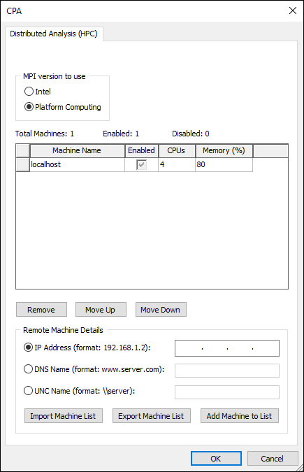
Select Local analysis or Distributed analysis. If users select Distributed analysis, click Configure to open the CPA window and set up remote machines.
-
Once remote machines are set up, click OK to return to the CPA Options window.
-
Choose whether to check Perform ERC during simulation setup (abort when an electrical short is detected). The ERC (Electrical Rule Check) will analyze the design for shorted nets and abort the simulation if shorts are detected. If the box is not checked, the design may detect shorts and will notify users in the Information/Errors/Warnings window, but the simulation will continue. If appropriate, also check Exclude non-functional pads (checked by default). Doing so will exclude non-functional nets from ERC.
-
Select the Advanced tab.
-
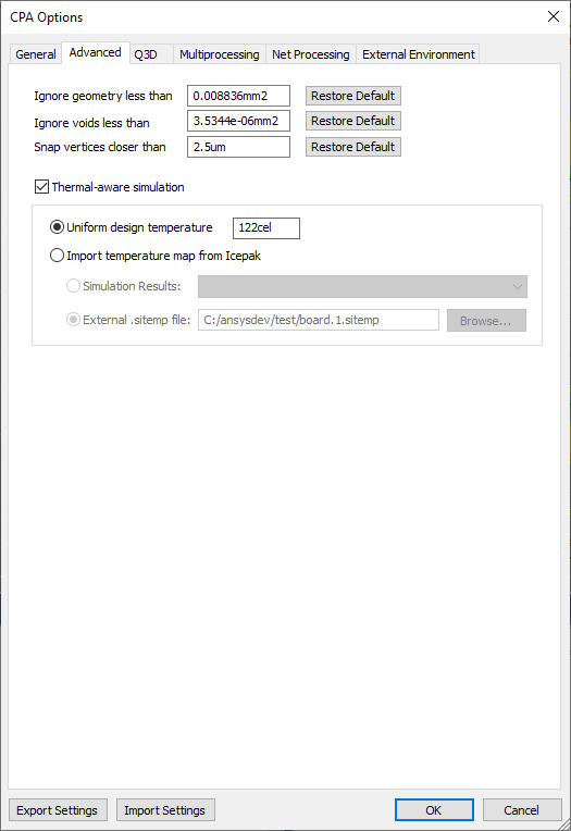
Enter a value in the Ignore geometry less than box. Geometry with an area (after being combined with any overlapping geometry) below this specified threshold is ignored during simulation.
- Enter a value in the Ignore voids less than box. Voids whose area (after being combined with any overlapping geometry) falls below this specified threshold is ignored during simulation.
Note:
Ansys recommends using the default settings. Refer to Advanced Geometry Processing Options.
- Enter a value in the Snap vertices closer than box. Entities and vertices that are separated by less than the distance specified in this box may be snapped together during solver pre-processing.
- Check the Thermal-aware simulation box to activate the corresponding options (i.e., step 17).
- Select Uniform design temperature or Import temperature map from Icepak.
Uniform design temperature - sets a global design temperature. Also used to modify the conductivity of metallization during DC IR simulation (i.e., in general, a higher temperature aserts a lower conductivity, implying a higher resistance). Enter a value in Celsius in the field (e.g., 122cel). Temperatures below absolute zero cannot be simulated (e.g., -273.15cel).
Import temperature map from Icepak - choose Simulations Results and select an Icepak temperature distribution file (i.e., a sitemp file) from the drop-down menu (e.g., Icepak Sim 1), or choose External .sitemp file, then Browse to an appropriate directory and select a saved or exported .sitemp file (e.g., c:/ansysdev/test/board.1.sitemp). The temperature data is used to locally adjust DC conductivity.
Note:Temperature modifiers (selected per material for the project) must be defined before launching a thermal aware simulation or the CPA simulation will complete without temperature dependence. Completing a DC IR simulation, then an Icepak simulation before a CPA simulation is the simplest path. Refer to Computing DC IR Simulations and Computing Icepak Simulations.
-
Select the Q3D tab.
-
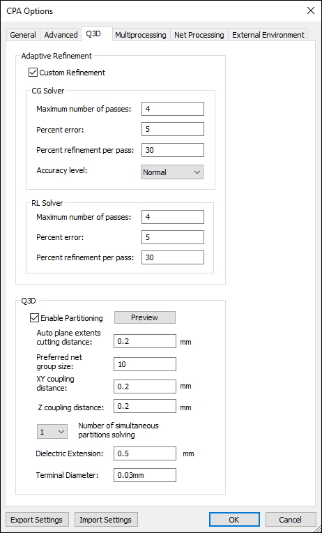
From the Adaptive Refinement area, check the Custom Refinement box to activate the CG Solver and RL Solver areas.
- Enter the following CG Solver and RL Solver parameters:
- Maximum number of passes and Percent error - specify stopping criteria. SIwave exits the adaptive loop as soon as one of these criteria is satisfied.
- Percent refinement per pass - specify what percentage of high-error triangles should be refined during each iteration.
- Accuracy Level - select Normal or High from the drop-down menu. If Normal is selected, the solver will give accurate results for most applications. If High is selected, the solver provides greater accuracy at the expense of speed and memory.
-
From the Q3D Partitioning area, check the Enable Partitioning box and specify the following options (refer to Partitioning Algorithm and CPA Modeling Using Partitioning):
- Auto plane extents cutting distance – determines how much of the power and ground nets is included in each partition. Portions within this distance from the partition's signal nets are included.
- Preferred net group size – when possible, the number of nets in each partition will be close to this amount.
- XY coupling distance – sets the distance in the XY plane that governs whether two nets are considered coupled.
- Z coupling distance – sets the distance in the Z direction that governs whether two nets are considered coupled.
- Number of simultaneous partitions solving – for local analysis, select the number of processors solving partitions simultaneously from the drop-down menu.
- Dielectric Extension – defines how much additional dielectric material should be added surrounding each partition.
- Terminal Diameter – defines the size of sources and sinks for RL extraction, except those defined on solderballs and bumps. For sources and sinks defined on solderballs/bumps, the respective diameters of the solderballs/bumps are used to set the sizes. This option is not applicable if the selected Model Type is RDL/IC.
- Select the Multiprocessing tab.
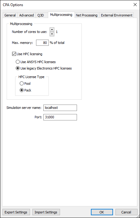
- Set the Number of cores to use when computing the solution. This feature is available only if users purchased the multiprocessing or HPC license option for SIwave.
- Enter a value in the Max. Memory field to set the memory used as a percentage of total RAM. This option is only available if Use HPC licensing is selected (i.e., step 24.).
- Check the Use HPC licensing box to enable shared memory multiprocessing.
- Select Use Ansys HPC licenses or Use legacy Electronics HPC licenses.
Note:
The option to choose a license type (either Ansys HPC or Electronics HPC) is not available when SIwave is running in Pro/Premium/Enterprise licensing mode.
- From the HPC License Type area, select Pool to use HPC licenses for distribution or Pack to use HPC Pack licenses.
- Enter the name or IP address of the simulation server in the Simulation server name field.
- Enter the Port number. See: Remote Solve for details on setting up for remote solves.
- Select the Net Processing tab.
-
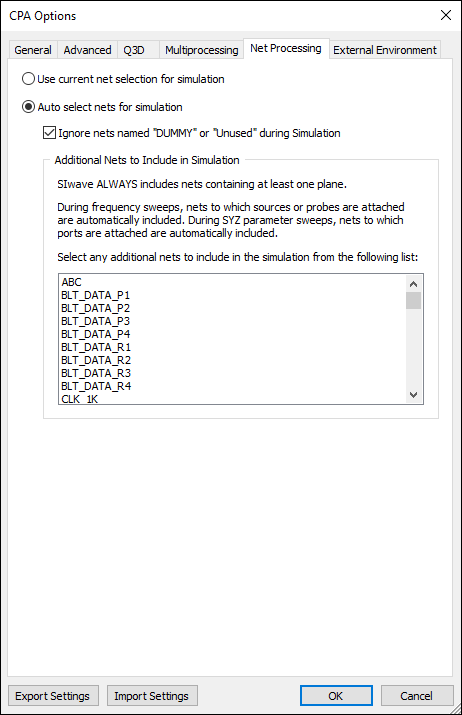
Select use current net selection for simulation to run a simulation including only the nets that are selected in the Nets workspace. Otherwise, leave the default setting of Auto select nets for simulation.To include dummy/unused nets in the simulations, clear the Ignore nets named "DUMMY" or "Unused" during Simulation check box. By default, these nets are ignored.
- Select the External Environment tab.
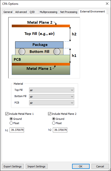
- From the Material area, use the Top Fill, Bottom Fill, and PCB drop-down menus to select materials.
- Check the Include Metal Plane 1 and/or Include Metal Plane 2 boxes to add up to two metal planes to the model. This option is applicable to the Q3D solver choice only. Metal Plane 1 represents the upper PCB Ground or VDD plane. Metal Plane 2 can represent a metal cover, a heat sink, or any other metal plane located above the package. This metal plane behaves similarly to Metal Plane 1.
- For each selected metal plane, select Ground or Float.
- Ground - uses the metal plane as part of the return path. This configuration affects the inductance and capacitance of the package nets.
- Float leaves the metal plane floating. This configuration affects only the capacitance of the package nets.
- For each selected metal plane, enter a value for height.
- h1 - distance from the bottom layer of the package stackup to the top of Metal Plane 1. The solder balls included in this space add to the inductance and capacitance effects on the package nets.
- h2 - distance from the top layer of the package stackup to the bottom of Metal Plane 2.
- Click OK to save CPA options and exit the CPA Options window.
CPA Control XML File
Use a cpa_control.xml file to set other options. This file should be placed in the same folder as the *.siw project file.
A sample file is shown below:
<?xml version="1.0" encoding="utf-8"?>
<!-- Individual sections can be disabled by setting Enable=No -->
<CPA_Control_Specs>
<!-- If enabled, the annotated ploc file would use this chip layer name -->
<Chip_Layer_Name Enable="yes" Name="ic_m1_layer">
<!-- All units in mm and are in package DIE coordinates -->
<!-- Only the die pins (having PLOC connections) falling within this polygon region are extracted -->
<Partial_DIE_Region Enable="no">
<Point x="-5.0" y="5.36"/>
<Point x="-5.0" y="0.37"/>
<Point x="5.5" y="0.37"/>
<Point x="5.5" y="5.36"/>
</Partial_DIE_Region>
<Partial_DIE_Region Enable="no">
<Point x="-5.0" y="5.36"/>
<Point x="-5.0" y="0.37"/>
<Point x="5.5" y="0.37"/>
<Point x="5.5" y="5.36"/>
</Partial_DIE_Region>
<Partial_DIE_Region Enable="no">
<Point x="-5.0" y="5.36"/>
<Point x="-5.0" y="0.37"/>
<Point x="5.5" y="0.37"/>
<Point x="5.5" y="5.36"/>
</Partial_DIE_Region>
<!-- Voltage values are in volts -->
<!-- The unconnected PLOC pins corresponding to these Chip nets are terminated with voltage supplies -->
<Open_PLOCpins_VoltageSupply Enable="no">
<Net Name="NewNet1" Voltage="1.2847"/>
<Net Name="NewNet2" Voltage="2.384"/>
</Open_PLOCpins_VoltageSupply>
</CPA_Control_Specs>
