Computing DC IR Simulations
DC IR analysis solves for the voltage drop across the power plane. The DC solution provides important information pertaining to power delivery, including:
- Status of the voltage regulator to determine if it is functioning and supplying the proper DC voltage to all active components attached to power rails
- DC current density information to warn where board or via damage may occur
SIwave makes use of a dedicated DC solver that is based on a well-known formulation and produces an efficient DC solution.
SIwave can perform the following actions:
- Compute DC voltage and current density for a given source configuration
- Compute IR-drop and current flow within each element in a PCB model (resistor, inductor, via, trace, plane, bondwire, source, etc.)
- Perform adaptive mesh refinement for increased accuracy
The DC IR simulation provides a connection to the thermal solver Ansys Icepak. If appropriate, export the DC IR data to Icepak after analysis, or import a temperature map from Icepak to use in the DC IR simulation.
As a preliminary step, users may want to define equipotential regions.
Users can configure component parameters prior to simulation from the SIwave Workflow Wizard or skip directly to Setting Up the Compute DC Current and Voltage Distribution Window.
Beginning Simulation From the SIwave Workflow Wizard
Complete the following steps to begin configuring a simulation from the SIwave Workflow Wizard.
-
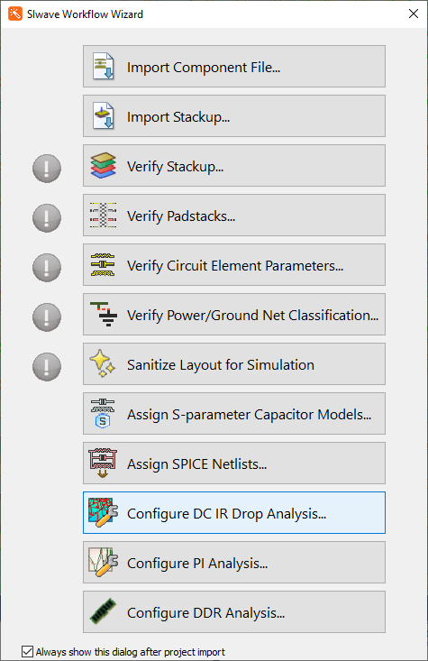
From the SIwave Workflow Wizard, select Configure DC IR Drop Analysis to open the DC IR Configuration window.
-
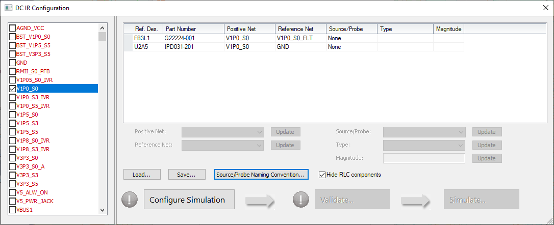
From the list on the left, check the box adjacent to an appropriate net (e.g., V1P0_S0).
-
From the table, do the following:
-
Make selections from the Source/Probedrop-down menu (i.e, select None, Current Source, Voltage Source, Voltage Probe, or Terminal) .
-
The Type drop-down menu is enabled if Current Source or Voltage Probe are selected from the Source/Probe drop-down menu. Select either Constant Voltage (i.e., adding one circuit element) or Distributed Current (i.e., adding a circuit element on every pin) from the Type drop-down menu.

-
Enter a Magnitude in the field or accept the default parameter, if any.
-
Select the left-most empty cell in the component's row to populate the fields beneath the table. Then make further adjustments, as appropriate.

-
-
Click Configure Simulation.
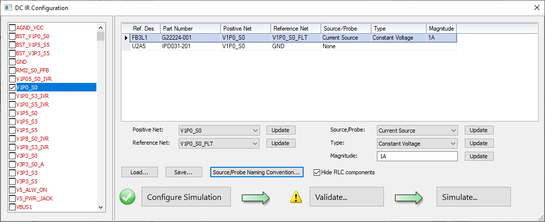
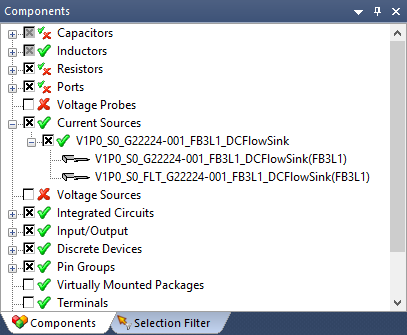
The Components window will populate with an appropriate sources/probes.
-
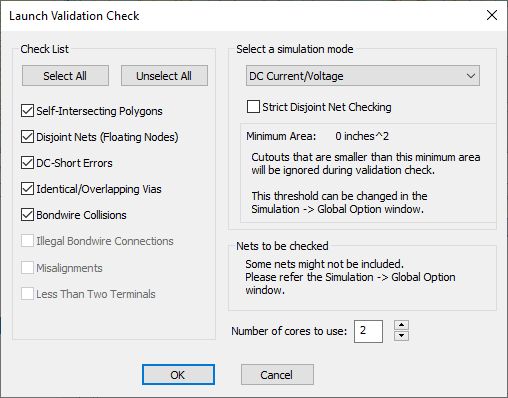
Click Validate to open the Launch Validation Check window.
-
If appropriate, configure the validation check. Then click OK to begin validation. View progress in the Process Monitor (Validation Checker).

-
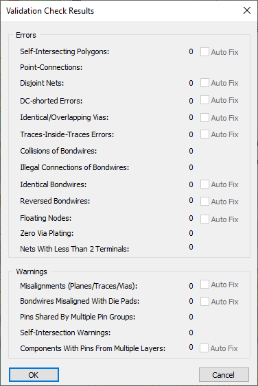
After the validation check is complete, a Validation Check Results window appears. Assuming the simulation has passed validation, click OK to return to the DC IR Configuration window.
-
Click Simulate to open the Compute DC Current and Voltage Distribution window.

-
Continue to step 2 of Setting Up the Compute DC Current and Voltage Distribution Window.
Setting Up the Compute DC Current and Voltage Distribution Window
Complete the following steps to finalize simulation solver setup and run a simulation.
- From the Simulation tab, click Compute DC IR to open the Compute DC Current and Voltage Distribution window.

DC thermal information is provided when requested for use in Icepak simulations using a full-resolution meshed power map.
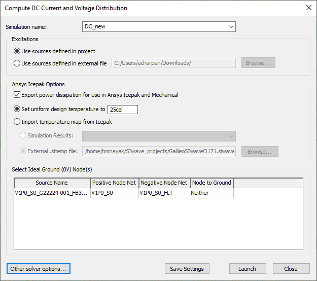
- From the Simulation Name field, enter a name for the DC IR simulation.
- From the Ansys Icepak Options area:
- Check Export power dissipation... if users want to export data to Ansys Icepak or Mechanical.
- Select either:
- Set uniform design temperature... and enter a value, in celsius. This sets a global design temperature and is used to modify the conductivity of metallization during the DC IR simulation. In general, the higher the temperature, the lower the conductivity (implying a higher resistance).
- Import temperature map... and select an Icepak temperature distribution file, either from a previous simulation or from an external *.sitemp file. The temperature data can locally adjust DC conductivity.
Resistivity of conductors is adjusted by:

Where:
- R is the conductor resistance at temperature T.
- Rref is the conductor resistance at reference temperature Tref.
- α is the temperature coefficient of resistance for conductor material (4e-3 per degree Celsius for all materials in SIwave).
- T is the conductor temperature in degrees Celsius.
- Tref is the reference conductor temperature in degrees Celsius at which the resistivity of a metal in the material definition is assumed to be taken (20 degrees Celsius in SIwave).
- From the Select Ideal Ground Node(s) area, choose a ground node from the table. Select a current or voltage source at 0 volts (ideal ground). All other voltages are computed with respect to this node. If no ideal ground node is selected, SIwave automatically picks a source terminal to ground.
- Use the Node to Ground drop-down menu to select Neither, Negative, or Positive.
- Click Save Settings.
- To view additional solver options, click Other solver options.
- Click Launch to begin the simulation.
View progress in the Process Monitor.

If users select Negative on a voltage source, the voltage display on its ground pin will be 0 V.
If users select Positive on a voltage source, the voltage display on its ground pin will be negative.
Consider this as being the 0 node in a SPICE simulation. This is the node to which all voltages should be referenced. Since SIwave includes the return paths of all planes (including the ground), we cannot assume that all of the sources reference that 0 node. Thus we have to pick one to be the absolute 0 node reference. So if we put the 0 node on the positive side of a voltage plane, the "ground" or return path would show as negative.
If the simulation is canceled while it is running, and even if one iteration has been completed, the last refinement iteration will display.
