Computing DC IR Simulations in HFSS 3D Layout
DC IR analysis solves for the voltage drop across the power plane. The DC solution provides important information pertaining to power delivery, including:
- Status of the voltage regulator to determine if it is functioning and supplying the proper DC voltage to all active components attached to power rails
- DC current density information to warn where board or via damage may occur
HFSS 3D Layout makes use of the SIwave DC solver that is based on a well-known formulation and produces an efficient DC solution.
Thermal modifiers are expressions that evaluate the conductivity of metals as a function of temperature. If such expressions have been specified in the material manager for metals that are used in the design, they are respected during SIwave DC simulations. If no such expressions have been explicitly specified, the SIwave DC solver uses the following to derate the resistivity of metals as a function of temperature:
resistivity = rho_0 * (1 + 0.004 * (Temp - T0))
where: rho_0 is the metal's resistivity measured at a temperature of T0 = 20 deg C.
HFSS 3D Layout can perform the following actions:
- Add current sources, voltage sources, voltage probes, and DC terminals
- View and create Voltage Regulators (VRMs)
- Define equipotential regions
- Compute DC current and voltage distribution
- Export DC IR simulation results
- Export DC IR data to Icepak, or import a temperature map from Icepak to use in the DC IR simulation
- Plot DC IR field overlays
- Overlay a DC Temperature Field
Users can configure component parameters prior to simulation from the SIwave Workflow Wizard or skip directly to Setting Up the Compute DC Current and Voltage Distribution Window.
Beginning Simulation From the SIwave Workflow Wizard
Complete these steps to begin configuring a simulation from the SIwave Workflow Wizard.
-
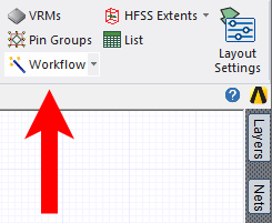
From the Layout tab, select Worfklow to open the SIwave Workflow Wizard window.
-
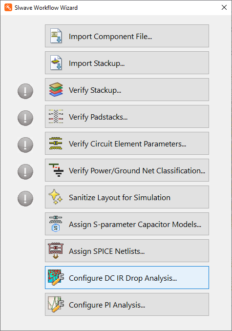
Click Configure DC IR Drop Analysis to open the DC IR Configuration window.
-
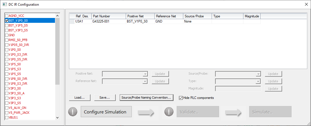
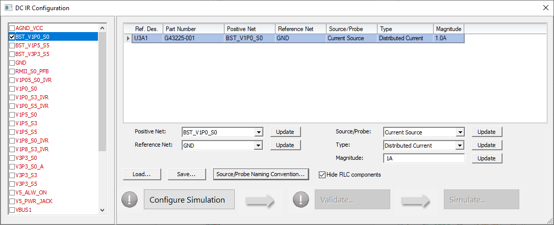
From the list on the left, check the box adjacent to a chosen net (e.g., BST_V1P0_S0).
-
From the table, do the following:
-
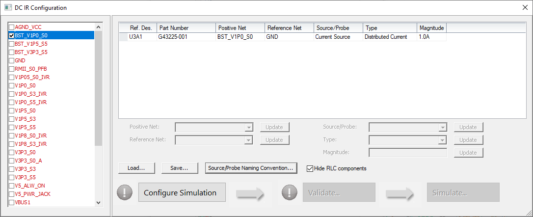
Make selections from the Source/Probe drop-down menu (i.e, select from None, Current Source, Voltage Source, Voltage Probe, or Terminal) .
-
The Type drop-down menu is enabled if Current Source or Voltage Probe are selected from the Source/Probe drop-down menu. Select either Constant Voltage (i.e., adding one circuit element) or Distributed Current (i.e., adding a circuit element on every pin) from the Type drop-down menu.
-
Enter a Magnitude in the adjacent field or accept the default parameter, if any.
-
Select the left-most empty cell in the component's row to populate the fields beneath the table. Then make further adjustments, as appropriate.
-
-
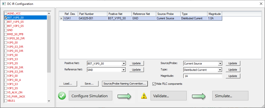
Click Configure Simulation.
-
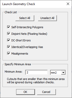
Click Validate to open the Launch Geometry Check window.
-
If appropriate, configure the validation check. Then click OK to begin validation. View progress in the Progress window.
 Note:
Note:Users will need to open the Progress window and position it conveniently beforehand.
-
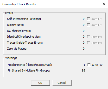
After the validation check is complete, a Geometry Check Results window appears. Assuming the simulation has passed validation, click OK to return to the DC IR Configuration window.
-
Click Simulate to open the Compute DC Current and Voltage Distribution window.

-
Continue to step 2 of Computing DC IR Simulations in HFSS 3D Layout .
Setting Up the Compute DC Current and Voltage Distribution Window
Complete these steps to finalize simulation solver setup and run a simulation computing DC current and voltage distribution.
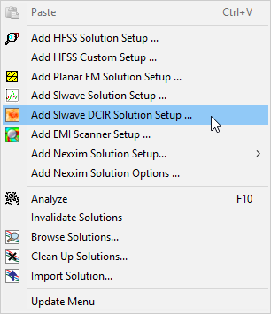
- From the Project Manager window, expand the Project Tree and [Active Design Folder]. Then right-click Analysis and select Add SIwave DCIR Solution Setup to open the Compute DC Current and Voltage Distribution window.
- From the Simulation Name field, enter a name for the DC IR simulation.
- From the Ansys Icepak Options area, there are two optional settings:
- Check Export power dissipation to export data to Ansys Icepak.
- Check Import temperature map to select an Icepak SIwave temperature distribution file (*.sitemp). The temperature data can locally adjust DC conductivity.
- From the Select Ideal Ground Node(s) area, select a ground node on the table. Select a current or voltage source at 0 volts (ideal ground). All other voltages are computed with respect to this node. If no ideal ground node is selected, HFSS 3D Layout automatically picks a source terminal to ground.
- Click the Node to Ground drop-down menu to select Neither, Negative, or Positive.
- To view additional solver options, click Other solver options.
The SIwave Solution Setup window opens, on the DC tab.
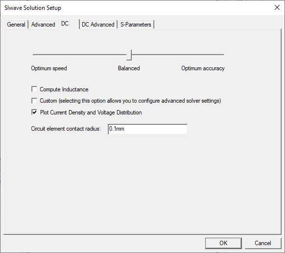
From this window, do the following:
- Use the slider to balance speed and accuracy:
- Optimum Speed – all options in the DC Advanced tab are deactivated.
- Balanced – the Mesh Bondwires and Mesh Vias options are selected, along with adaptive Mesh Refinement.
- Optimum Accuracy – the mesh are refined on bondwire and vias, and more aggressive refinement parameters are specified.
- Select whether to Compute Inductance. The inductance is computed by integrating the vector potential at DC using an efficient, multi-level fast multipole method with two-level parallelization. In some cases, this may require significant computational time and memory.
- Select whether to use Custom simulation settings.
- Select whether to Plot Current Density and Voltage Distribution. Clear this check box to save disk space if users do not need to post-process voltage and current plots (e.g., if the user only want to export a SPICE netlist after a DC simulation, it might not be helpful to save any field data to disk).
- Enter the Circuit Element Contact Radius. Equal potential is enforced in the contact radius, and no mesh refinement is done inside the contact region.
- Use the slider to balance speed and accuracy:
- Check Custom to enable DC Advanced settings, then select the DC Advanced tab.
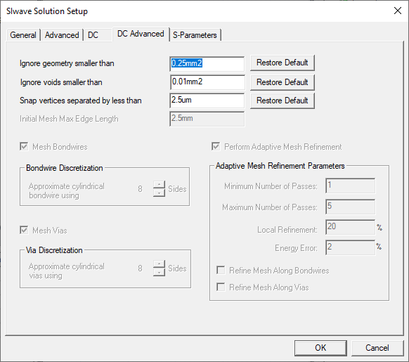
DC Advanced options include:
- Ignore geometry smaller than – geometry whose area (after being combined with any overlapping geometry) falls under this specified threshold is ignored during simulation.
- Ignore voids smaller than – geometry whose area (after being combined with any overlapping geometry) falls under this specified threshold is ignored during simulation.
- Snap vertices separated by less than – entities (e.g., vias) and vertices that are separated by less than the distance specified in this box may be snapped together during solver pre-processing.
- Initial Mesh Max. Edge Length – specifies the maximum edge length chosen in the mesh (before any adaptive refinement occurs).
- Mesh Bondwires – check if users do not want to model bondwires as point connections to mesh. Specify the Bondwire Discretization (the number of sides used to approximate cylindrical bondwires). Specify any value between 6 and 64. The default value is 8.
- Mesh Vias – check if users do not want to model vias as point connections to mesh. Specify the Via Discretization (the number of sides used to approximate cylindrical vias). Specify any value between 6 and 64. The default value is 8.
- Perform Adaptive Mesh Refinement – check to perform Adaptive Mesh Refinement, and populate the fields:
- Minimum Number of Passes – an adaptive analysis does not stop unless the minimum number of passes specified has been completed, even if convergence criteria have been met.
- Maximum Number of Passes –
this value is the maximum number of mesh refinement cycles users want
the simulation to perform. This value is a stopping criterion for the adaptive
solution. If the maximum number of passes has been completed, the adaptive
analysis stops; otherwise, the adaptive analysis continues unless the
convergence criteria are reached.
Note:
The size of the finite element mesh — and the amount of memory required to generate a solution — increases with each adaptive refinement of the mesh. Setting the maximum number of passes too high can result in Electronics Desktop requesting more memory than is available or taking excessive time to compute solutions.
- Local Refinement – this value determines how many triangles are added at each iteration of the adaptive refinement process. The triangles with the highest error is refined. The default value is 20%.
- Energy Error – the default value is 2%.
- Refine Mesh Along Bondwires – check to refine mesh along bondwires.
- Refine Mesh Along Vias – check to refine mesh along vias.
- Select the S-Parameters tab.
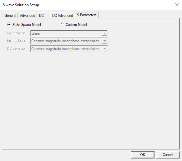
- Select State Space Model or Custom Model. If Custom Model is selected, set the following options:
- Interpolation – select Point, Linear, or Step from the drop-down menu.
- Extrapolation – select Zero padding, Same as last point, Linear extrapolation from last 2 points, or Constant magnitude linear phase extrapolation from the drop-down menu.
- DC Behavior – select Zero padding, Same as last point, Linear extrapolation from last 2 points, or Constant magnitude linear phase extrapolation, Series Capacitor, or Leave all signal lines open circuited from the drop-down menu.
Note:Refer to the following pages for an example of using the SIwave Solution Setup window to change S-Parameters or using a preconfigured Python script to generate an Ansys ECAD database file, which can then be imported into Electronics Desktop to create a custom SIwave setup.
- After making any chosen changes, click OK to exit the solution setup.
- Click OK to save the solution setup.
The Project Manager window updates to show the DC IR setup under Analysis.
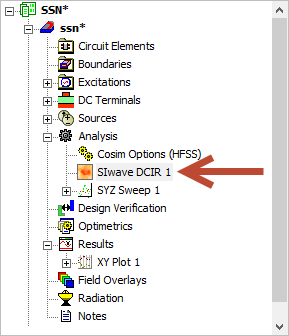
- Run through the SIwave Workflow Wizard.
- From the Project Manager window, right-click the analysis and select Analyze.
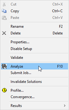
- The Progress window displays the simulation's progress. When it finishes, view or export results.
If users select Negative on a voltage source, the voltage display on its ground pin is 0 V.
If users select Positive on a voltage source, the voltage display on its ground pin are negative.
Consider this as being the 0 node in a SPICE simulation. This is the node to which all voltages should be referenced. Since HFSS 3D Layout includes the return paths of all planes (including the ground), do not assume that all the sources reference that 0 node. Thus, pick one to be the absolute 0 node reference. So if the 0 node is on the positive side of a voltage plane, the "ground" or return path is shown as negative.
