SIwave Workflow Wizard in HFSS 3D Layout
The SIwave Workflow Wizard walks you through the steps to make a project ready for SIwave simulations. Complete these steps to access the wizard.
-
From the Layout tab, click Workflow to open the SIwave Workflow Wizard window.

-
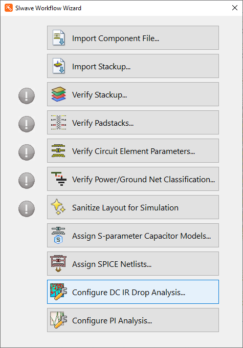
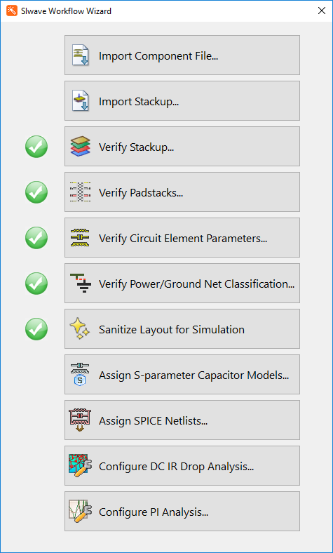
Steps with an exclamation point next to them should be completed before running any SIwave simulations in HFSS 3D Layout. Other steps may be appropriate, depending on the simulation type. Once completed, the exclamation points turn into green check marks.

SIwave Workflow Wizard steps include:
- Import Component File – allows you to import component files (*.cmp) generated by third-party layout tools so you do not have to re-draw components while transferring the design. These files contain detailed pin information for discrete devices, input/output devices and integrated circuits.
- Import Stackup – allows you to import a stackup from an Extensible Markup Language (*.xml) file or layer stackup file (*.stk). PCB/package designs are often based on the same stackup. Stackup file import/export allows you to define the exact parameters (set materials, layer thicknesses, etc.) for a particular stackup once, and have these assignments be reapplied consistently across different designs.
- Verify Stackup – opens the Edit Layers window / Layer Stackup Wizard so that you can verify the layers and materials used in the design.
- Verify Padstacks – opens the Padstack Instances window, where you can verify or edit padstacks.
- Verify Circuit Element Parameters – opens the DC Simulation Element Data window, where you can verify settings for Capacitors, Inductors, Resistors, Ports, Current Sources, Voltage Sources, and Net Terminals.
- Verify Power/Ground Net Classification – allows you to specify Power/Ground Nets and Non Power/Ground Nets.
- Sanitize Layout for Simulation – performs an operation for cleaning power and ground nets in order to fix certain alignment problems and complexities that may slow down simulation. This works by uniting the planes and traces for each net to be cleaned. Once the united planes are formed, portions that display trace-like properties are converted into traces. Under certain conditions, these traces are extended in order to improve their connection with vias, pads, and the remaining planes. Lattices originally formed from multiple traces become planes with cutouts after the sanitization process.
- Assign S-parameter Capacitor Models – opens the SPICE/S-parameter Vendor Component Management window, where you can assign SPICE/S-parameter models to components.
- Assign SPICE Netlists – opens the RLC SPICE Model Setup window, where you can attach SPICE models to components.
- Configure DC IR Drop Analysis – opens the DC IR Configuration window, a step in running DC IR simulations.
- Configure PI Analysis – opens the PI Configuration window for running the SIwave SYZ Solver.
