This section describes the detailed modeling of the PCB assembly. The following modeling topics are covered:
The assembly consists of three PCBs stacked together. Each PCB consists of a
circuit board with IC packages on top. The board is a 0.20m×0.28m rectangular
surface body with a 1 mm uniform thickness. The IC packages are 3D structures, each
with a thickness of 5 mm. The board is modeled with
SHELL181, which is suitable for analyzing thin to
moderately thick shell structures. The IC packages are modeled with
SOLID186, which is a 3D 20 node solid element,
exhibiting quadratic displacement behavior. The stack is connected together by five
vertical columns. These are thick beam structures (length/diameter  10), and they are modeled using BEAM188.
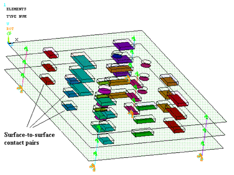
BEAM188 uses Timoshenko beam theory, which includes shear-deformation effects, and is one of the most accurate beam elements for analyzing moderately stubby beam structures. A hexahedral dominant mesh is used to mesh the board and the solids, resulting in each PCB having 14600 nodes. Both the board and the IC packages are made of polyethylene material. The supporting columns are made of aluminum alloy. The total number of nodes for the model is 44097 with 26046 elements.
Bonded and flexible surface-to-surface contact pairs are used to define the contact between the IC packages and the circuit board. Contact and target surfaces are used to connect the IC packages to the board. The contact surface is modeled with CONTA174 elements and the target surfaces are modeled using TARGE170 elements. The surface-to-surface contact elements have the following advantages over the node-to-node elements:
For each board, fifteen contact pairs are identified.