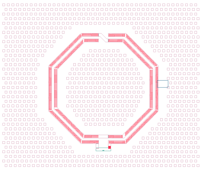
Via Snapping in IC Mode
Via groups serve as an electrical connection between objects on different metal layers. Sometimes objects and via groups are misaligned by a small amount which can increase mesh complexity. Snapping via groups aligns the objects and via groups across layers.
Complete steps in the following subsections to configure Via Snapping settings, then snap (i.e., align) vias within a design.
Configuring Via Snapping Settings
- From the Layout ribbon, click Settings.
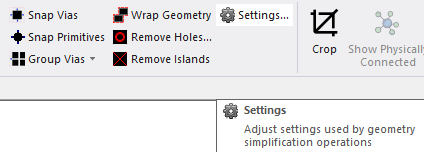
The Geometry Simplification Settings window opens.
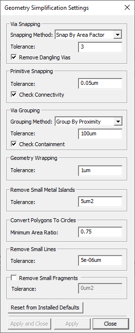
- From the Via Snapping area, do the following:
Select a Snapping Method from the drop-down menu (Snap By Area Factor selected by default).
- Snap By Area Factor - Via groups are snapped by a maximum area equal to the Tolerance times the surface area of the via group being snapped.
- Snap By Distance - Via groups are snapped by a maximum distance of the Tolerance.
- Enter a value in the Tolerance field (e.g., 3).
- Check the Remove Dangling Vias box to delete vias that have no connectivity or have connectivity only to a single layer (checked by default).
- Click Apply and Close.
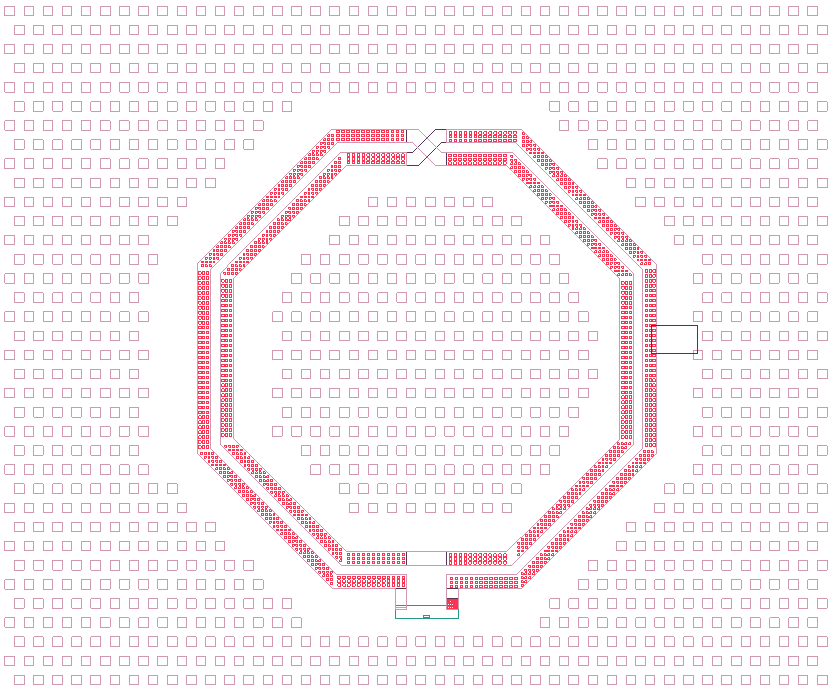
Snapping Vias on a Specific Layer
-
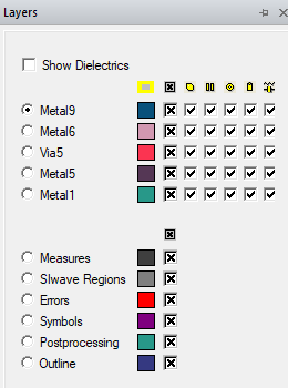
If the Layers window is not visible, navigate to the Layers tab. Click the Layers tab to open the window.
-
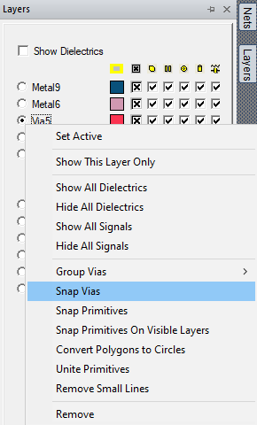
Right-click the chosen layer (e.g., Via5) and select Snap Vias.
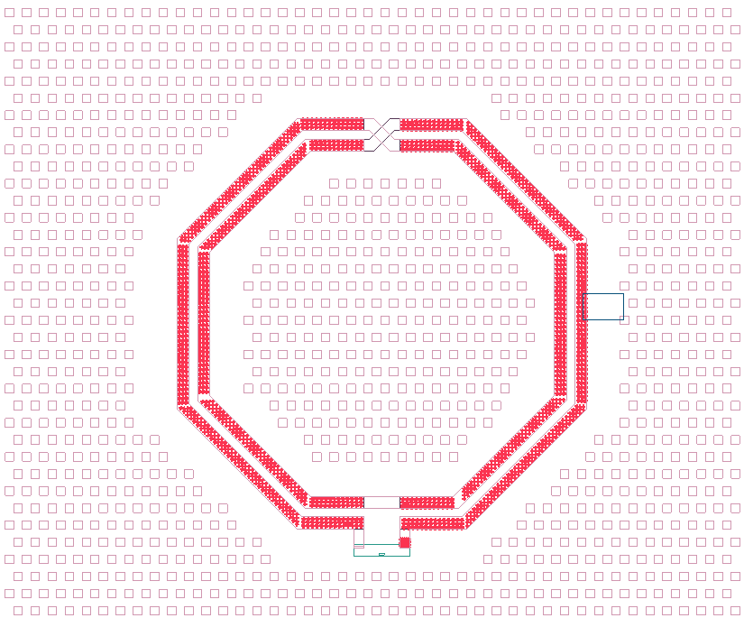
The vias in the design are aligned.
Snapping Vias in the Layout Editor
- From the Layout Editor, select a group of via primitives.
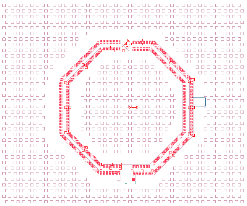
- From the Layout ribbon, click Snap Vias.
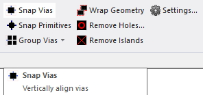
The selected vias are aligned.
