VM-WB-MECH-109
VM-WB-MECH-109
Piezoelectric Rectangular Strip Under Pure Bending Load
Overview
| Reference: | Parton, V. Z., Kudryavtsev, B. A., & Senik, N. A. (1990). Applied Mechanics: Soviet Review, Vol. 2: Electromagnetoelasticity. CRC Press. |
| Solver |
Ansys Mechanical |
| Analysis Type(s): | Coupled Field Static |
| Element Type(s): |
2D Plane Stress |
Test Case
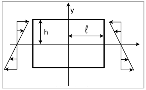
A piezoceramic (PZT-4) rectangular strip occupies the region |x| ≤ ℓ, |y| ≤ h. The material is oriented such that its polarization direction is aligned with the Y axis. The strip is subjected to the pure bending load σx = σ1y at x = ± ℓ. Determine the electro-elastic field distribution in the strip.
This test case is also solved using Ansys Mechanical APDL. See VM231.
| Material Properties | Loading |
|---|---|
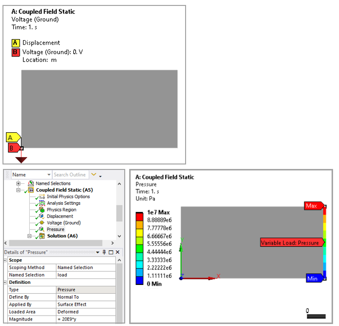
| ℓ = 1 mm and h = 0.5 mm | Pressure Slope = -20 N/mm3 |
Materials Properties Tables
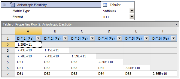
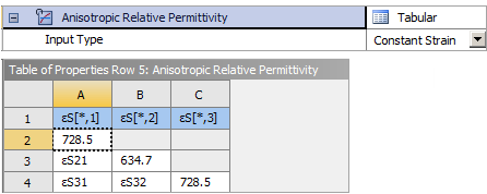
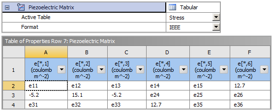
The piezoelectric material properties of PZT4 defined in Engineering Data are given below:
Analysis Assumptions and Modeling Notes
The finite element model uses a single 8-node, 2-D quadrilateral element (PLANE223).
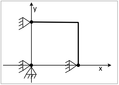
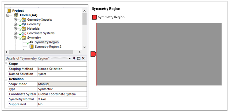
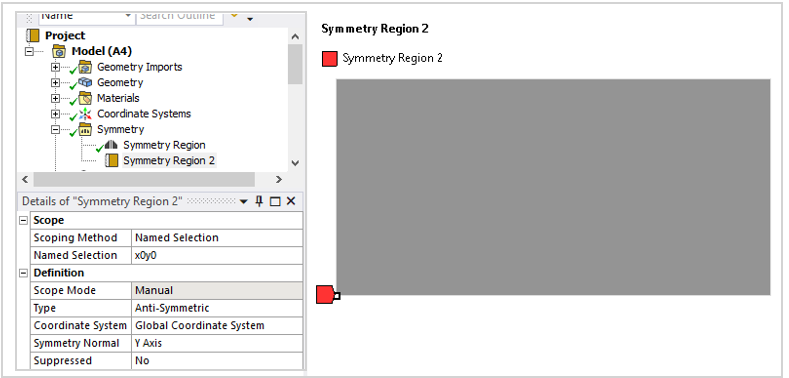
Only a one-quarter symmetry sector of the rectangular strip is modeled. Symmetric and antisymmetric boundary conditions are applied as shown below.
Results Comparison
The Workbench results are compared with target specified in reference book.
| Result at Node 3 | Target | Workbench App | Error (%) |
|---|---|---|---|
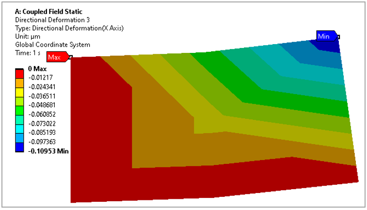
| Directional Deformation in X (µm) | -0.10953E-07 | -0.10953E-07 | 0.0 |
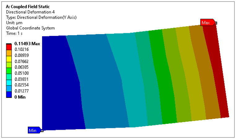
| Directional Deformation in X (µm) | 0.1493E-07 | 0.1493E-07 | 0.00 |
| Electric Voltage (V) | 27.379 | 27.379 | 0.000 |
| Equivalent Stress (N/mm2) | 10.000 x 10⁶ | 10 x 106 | 0 |
| Directional Electric Field Intensity in Y (V/m) | -109.515E-03 | -109.515E-03 | 0.00 |


