
Inserting an HFSS 3D Layout Design
This page briefly describes how to set up and run an HFSS 3D Layout design in the Electronics Desktop. The focus is on circuit and system analysis and the framework required to design RF-microwave, signal integrity, and printed circuit board applications. Before beginning, launch Electronics Desktop (Electronics Desktop), create a new project, and also enable the display of the Choose Technology window.
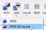
To insert an HFSS 3D Layout design:
- From the Project menu, select Insert HFSS 3D Layout Design or in the Desktop ribbon, open the menu under the HFSS icon and select HFSS 3D Layout to open the Choose Layout Technology window.
So long as the check box Show this window on new design is selected, this window appears when a new design is inserted into a project. If the check box is cleared, the next time that a new design is inserted, the window does not appear and a design is inserted using the chosen technology on the last insertion.
- Select an existing EM technology on the list or click None to manually add the model’s metal and dielectric layers.
A new design appears in the Project Manager window. The design is named HFSS3DLayoutn by default, where n is the order of the design in a potential series of designs. Folders named Data, Excitations, Analysis, Optimetrics, and Results automatically appear under the design name. These folders store data about the design.
To automatically insert an HFSS 3D Layout design when creating a new project, see General Options > Desktop Configuration to open the Layout view window. You can now create or edit the design layers in the Edit Layers window.
To expand the Project Tree and view specific data about the model such as its boundary assignments, click + to the left of the design icon in the Project Manager window.