The Q3D solution setup mirrors the capabilities of a simulation run using Q3D Extractor. Complete these steps to add a Q3D solution setup to a project in IC mode.
The Q3D solution setup is a beta feature in IC Mode only. Beta features must be activated prior to use. Refer to Activating the Q3D Solution Setup Beta Feature for instructions.
- Open the Q3D Solution Setup window by doing one of the following:
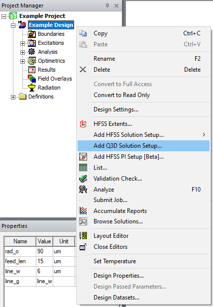
- From the Project Manager window, expand the Project Tree > [Active Design Folder] (e.g., Example Project > Example Design). Then right-click Analysis and select Add Q3D Solution Setup.
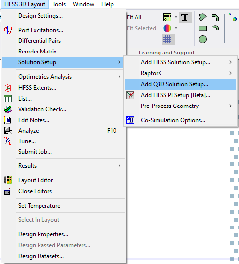
- From HFSS 3D Layout, select Solution Setup > Add Q3D Solution Setup.
- From the Project Manager window, expand the Project Tree > [Active Design Folder] (e.g., Example Project > Example Design). Then right-click Analysis and select Add Q3D Solution Setup.
-
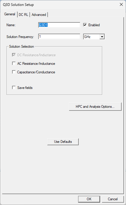
From the Q3D Solution Setup window, make selections from the visible tabs (i.e., by default, General, DC RL, and Advanced tabs are visible. CG and AC RL tabs appear depending on selections made in the General tab). Default values shown.
-
From the General tab, set the following:
-
Name – type a name in the field or accept the default.
-
Enabled – check the box to activate the setup.
-
Solution Frequency – enter a value in the adjacent field to specify the simulation frequency and select a unit of measurement from the corresponding drop-down menu.
-
DC Resistance/Inductance – checked by default; the solution setup will always solve and generate mesh for DC resistance and inductance.
-
AC Resistance/Inductance – check the box to solve and generate mesh for AC resistance and inductance; activates the AC RL tab.
-
Capacitance/Conductance – check the box to solve and generate mesh for DC capacitance and conductance; activates the CG tab.
-
Save fields – check the box to save the current settings as the new default settings.
-
HPC and Analysis Options – click to open the HPC and Analysis Options window. Refer to Setting HPC and Analysis Options.
-
- Click the DC RL tab.
-
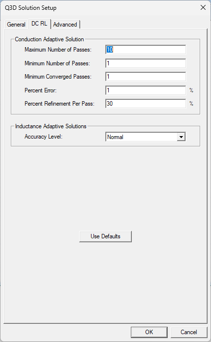
From the DC RL tab, set the following DC resistance/inductance options:
-
Maximum Number of Passes – enter a value in the adjacent field to specify the maximum number of mesh refinement cycles to perform. This value is a stopping criterion for the adaptive solution; the simulation continues until the maximum number of passes complete or convergence criteria are reached.
Important:The size of the finite element mesh — and the amount of memory required to generate a solution — increases with each adaptive refinement of the mesh. Setting the maximum number of passes too high can result in Electronics Desktop requesting more memory than available or taking excessive time to compute solutions.
-
Minimum Number of Passes – enter a value in the adjacent field to specify the minimum number of mesh refinement cycles. Simulation continues until after this number of passes complete.
Minimum Converged Passes – enter a value in the adjacent field to specify the minimum number of passes that must meet convergence criteria before the simulation stops.
-
Percent Error – enter a value in the adjacent field to specify an appropriate solution accuracy. Larger values produce solutions faster, but with less accurate results.
-
Percent Refinement Per Pass – enter a value in the adjacent field to specify how many tetrahedra are added at each iteration of the adaptive refinement process. The tetrahedra with the highest error are refined (e.g., entering 10 causes the mesh to increase approximately 10% each pass. If the mesh consisted of 1000 elements, the tetrahedra are refined such that 100 new elements are added to the mesh). The default percentage works well for most applications.
Note:A growth rate lower than the maximum occurs when there are not enough high error elements to warrant adaption. This reduces memory usage without sacrificing accuracy.
-
Accuracy Level – select an inductance adaptive solution accuracy from the drop-down menu. The solver will give accurate results at the Normal setting for most applications. The High, Higher, and Highest options offer greater accuracy at the expense of speed and memory.
-
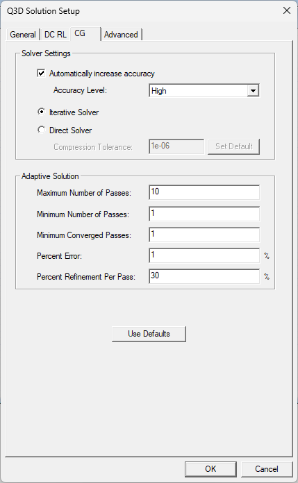
- If visible, click the CG tab.
-
From the CG tab, set the following DC capacitance/conductance options:
-
Automatically increase accuracy – check the box to automatically increase accuracy, then select an Accuracy Level from the drop-down menu. The solver will give accurate results at the Normal setting for most applications. The High, Higher, and Highest options offer greater accuracy at the expense of speed and memory.
-
Select either of the following:
-
Iterative Solver – check the box to activate the Iterative Solver, which is generally the fastest option. However, the Iterative Solver uses FMM compression, which may lead to slow convergence of GMRES iterations for poorly conditioned matrices.
-
Direct Solver – check the box to activate the Direct Solver, which has a higher setup time and uses more memory than the Iterative Solver. During setup, the Direct Solver performs an LU factorization of the FMM-compressed MoM system of equation. From the solution phase, each right hand side is solved using forward(L) and backward(U) substitutions. The Direct Solver converges quickly for poorly conditioned matrices and should only be used in cases requiring longer solution times (i.e., cases with extreme geometries and cases with more than 500 nets). After selection, enter a Compression Tolerance value. By default, the tolerance is 1e-6 for Normal or High accuracy, 1e-7 for Higher accuracy, and ie-8 for Highest accuracy. Setting a larger tolerance requires less setup time and memory, while setting a tighter tolerance requires more setup time and memory but leads to rapid convergence and faster solution time.
-
-
Maximum Number of Passes – enter a value in the adjacent field to specify the maximum number of mesh refinement cycles to perform. This value is a stopping criterion for the adaptive solution; the simulation continues until the maximum number of passes complete or convergence criteria are reached.
Important:The size of the finite element mesh — and the amount of memory required to generate a solution — increases with each adaptive refinement of the mesh. Setting the maximum number of passes too high can result in Electronics Desktop requesting more memory than available or taking excessive time to compute solutions.
-
Minimum Number of Passes – enter a value in the adjacent field to specify the minimum number of mesh refinement cycles. Simulation continues until after this number of passes complete.
Minimum Converged Passes – enter a value in the adjacent field to specify the minimum number of passes that must meet convergence criteria before the simulation stops.
-
Percent Error – enter a value in the adjacent field to specify an appropriate solution accuracy. Larger values produce solutions faster, but with less accurate results.
-
Percent Refinement Per Pass – enter a value in the adjacent field to specify how many tetrahedra are added at each iteration of the adaptive refinement process. The tetrahedra with the highest error are refined (e.g., entering 10 causes the mesh to increase approximately 10% each pass. If the mesh consisted of 1000 elements, the tetrahedra are refined such that 100 new elements are added to the mesh). The default percentage works well for most applications.
Note:A growth rate lower than the maximum occurs when there are not enough high error elements to warrant adaption. This reduces memory usage without sacrificing accuracy.
-
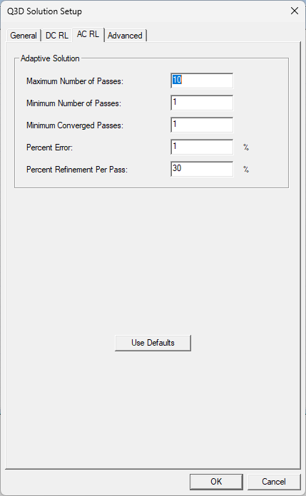
- If visible, click the AC RL tab.
-
From the AC RL tab, set the following AC resistance/inductance options:
-
Maximum Number of Passes – enter a value in the adjacent field to specify the maximum number of mesh refinement cycles to perform. This value is a stopping criterion for the adaptive solution; the simulation continues until the maximum number of passes complete or convergence criteria are reached.
Important:The size of the finite element mesh — and the amount of memory required to generate a solution — increases with each adaptive refinement of the mesh. Setting the maximum number of passes too high can result in Electronics Desktop requesting more memory than available or taking excessive time to compute solutions.
-
Minimum Number of Passes – enter a value in the adjacent field to specify the minimum number of mesh refinement cycles. Simulation continues until after this number of passes complete.
Minimum Converged Passes – enter a value in the adjacent field to specify the minimum number of passes that must meet convergence criteria before the simulation stops.
-
Percent Error – enter a value in the adjacent field to specify an appropriate solution accuracy. Larger values produce solutions faster, but with less accurate results.
-
Percent Refinement Per Pass – enter a value in the adjacent field to specify how many tetrahedra are added at each iteration of the adaptive refinement process. The tetrahedra with the highest error are refined (e.g., entering 10 causes the mesh to increase approximately 10% each pass. If the mesh consisted of 1000 elements, the tetrahedra are refined such that 100 new elements are added to the mesh). The default percentage works well for most applications.
Note:A growth rate lower than the maximum occurs when there are not enough high error elements to warrant adaption. This reduces memory usage without sacrificing accuracy.
-
- Click the Advanced tab.
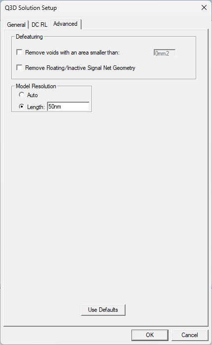
- From the Advanced tab, set the following:
Remove voids with an area smaller than – check the box to remove voids from the simulated primitives. Enter a tolerance value in the field. Voids smaller than the tolerance value will be removed.
Remove Floating/Inactive Signal Net Geometry – check the box to remove floating or inactive signal net geometry from the simulation.
Model Resolution – select either of the following:
Auto – the mesher calculates Model Resolution length based on each object's effective thickness. One mesh operation can be assigned to many objects, and each will be simplified based on its own dimensions.
Length – the mesher uses the specified Model Resolution length and unit of measurement.
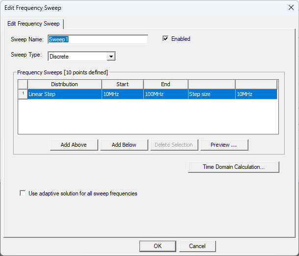
- Click OK to add the Q3D solution setup to the active design and simultaneously open the Edit Frequency Sweep window.Note:
For Q3D solution setups, the frequency sweep is only used to generate S parameters.
-
From the Edit Frequency Sweep window, click OK to accept the sweep with its default values or specify the following:
Note:The available tabs and options change with the selected sweep type.
-
Sweep Name – enter a name for the sweep.
-
Sweep Type – select Discrete or Interpolating:
-
Discrete – Generates field solutions at specific frequency points in a frequency range. Ideal when only a few frequency points are appropriate to accurately represent the results in a frequency range.
-
Interpolating – Estimates a solution for an entire frequency range. Ideal when the frequency range is wide and the frequency response is smooth. When Interpolating is selected, the Interpolation tab appears.
Note:The information specified for an Interpolating sweep dictates the amount of information that can be viewed on a post-processing plot.
-
-
Enabled – check to enable the sweep.
-
Frequency Sweeps area – use Add Above, Add Below, and Delete to add or remove sweeps. Each row in the table represents a separate sweep and each column is either a selectable parameter or a value field. You can add multiple frequency sweeps to the same setup. Specify the Start and End frequency for each sweep, and make selections from the additional options specific to the Distribution type.
-
Distribution – select from the following:
-
Linear Step – A linear range of frequency points for which users specify a constant step size. The simulation will solve the frequency point at each step in the specified frequency range, including the start and stop frequencies (e.g. , specifying 10 for the Start frequency, 20 for the Stop frequency, and 2.5 for the Step Size instructs the simulation to compute a solution for frequencies of 10, 12.5, 15, 17.5, and 20).
-
Single Point – Individual frequency points. Insert specific frequency points to solve in the frequency range after uniform frequency points. For Discrete sweep types only.
-
Linear Count – A linear range of frequency points for which users specify the number (count) of points within the frequency range. The simulation divides the frequency range into the count specified and solve each frequency point in the count.
-
Log Scale – A range of points for which users specify Start, End, and the number of Samples.The simulation assigns the sampled points using intervals based on a logarithmic scale.
-
-
-
Click Preview to view a preview of the sweep, as currently defined.

-
If the design includes dielectric layers exhibiting little variance in conductance (G) or capacitance (C) across frequency, check the Use adaptive solution for all sweep frequencies box to improve the speed and accuracy of the simulation.
-
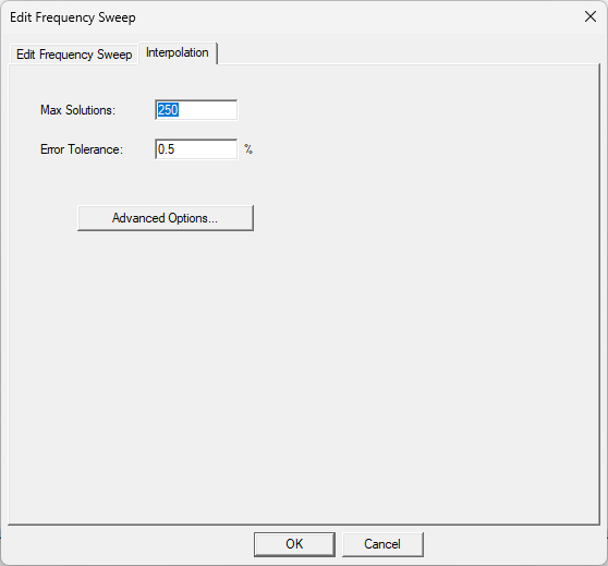
If Interpolating is selected from the Sweep Type drop-down menu, the Interpolation tab appears. Click the Interpolation tab.
-
From the Interpolation tab, specify the following:
-
Max Solutions – the maximum number of solutions that will be solved for the frequency range. The default is 250.
-
Error Tolerance – the maximum relative difference allowed between two successive interpolation solutions. The default is 0.5 percent.
-
-
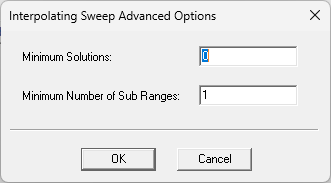
Click Advanced Options to open the Interpolating Sweep Advanced Options window.
-
From the Interpolating Sweep Advanced Options window, specify the following:
-
Minimum Solutions – the minimum number of converged solutions that will be solved for the frequency range (e.g., if this value is three, then once the sweep reaches convergence it simulates at two extra frequencies, resembling the minimum number of converged adaptive passes in a regular simulation). Setting a minimum number of solutions can eliminate non-physical S-parameter spikes. The default value is 0.
-
Minimum Number of Sub Ranges – the sub range number acts as an initial condition on the sweep to force initial even breakup of the null range into subranges. The end points and middle of each subrange will be solved, controlling the points at which the interpolating sweep is broken up and preventing redundant effort caused by neighboring interpolating sweeps solving the same point (e.g., 1 GHz-4 GHz and 4 GHz-9 GHz sweeps do not both solve the 4 GHz datapoint). The default value is 1.
-
-
Click OK to close the Interpolating Sweep Advanced Options window.
-
Click OK to close the Edit Frequency Sweep window and add any sweeps.
-
If any technology definition files were imported during the initial setup of the design, complete these steps to apply a technology definition before simulation.
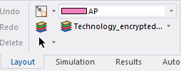
Note:If technology definition files were not imported during the initial setup of the design, users can add one or more files at any time before simulation. If a technology definition was applied during setup, the definition's name should already appear in the Layout ribbon adjacent to the Technology drop-down menu. Users will not need to complete these steps. Refer to Adding a Technology Definition File to a Design.
-
If a technology definition is available, navigate to the Layout ribbon and select Apply Technology from the Technology drop-down menu.

-
Once the Apply Technology window opens, select an appropriate technology definition file from the list and click OK.
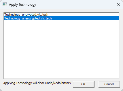
Once the technology definition is applied to the design, the definition's name appears adjacent to the Technology drop-down menu.
-
-
From the Project Manager window, right-click the Q3D solution setup (e.g., Q3D1) and select Analyze to run the simulation. Refer to Running Simulations.
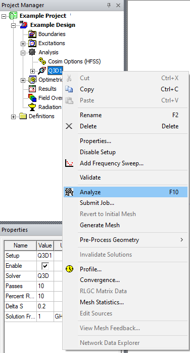
Electronics Desktop will begin simulation and generate an appropriate mesh. View, pause, or stop the simulation from the Progress window.

The Message Manager window will display pertinent information as the simulation progresses.

-
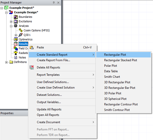
Once the simulation is complete, navigate to the Project Manager window and right-click Results to view the available Report options. Then select a report to open the Report window. Refer to Creating Reports.
-
There are several report options unique to Q3D solution setups. Refer to the following:
Sweep Solution
-
From the Solution drop-down menu, select Sweep.
-
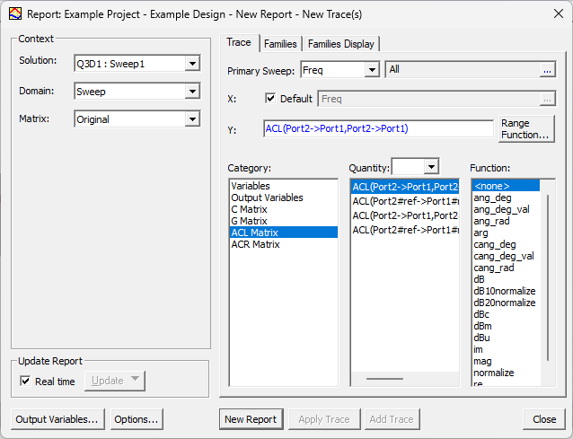
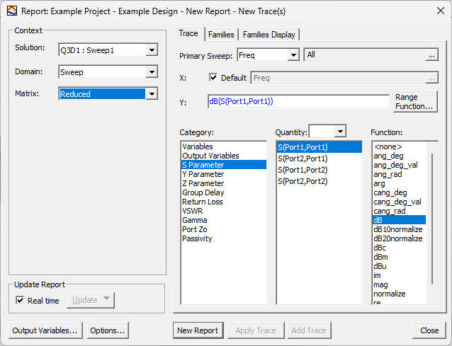
From the Matrix drop-down menu, select one of the following:
-
Original – populates the Category and Quantity list with C, G ACL and ACR matrices pertinent to the Q3D simulation.
-
Reduced – populates the Category list with parameters (e.g., S Parameter).
-
Last Adaptive Solution
From the Solution drop-down menu, select Last Adaptive to populate the Category and Quantity list with matrices pertinent to the Q3D simulation (i.e., C, G, DCL, DCR, ACL, and ACR).

Adaptive Pass Solution
-
From the Solution drop-down menu, select Adaptive Pass to populate the Category and Quantity list with matrices pertinent to the Q3D simulation (i.e., C, G, DCL, DCR, ACL, and ACR).
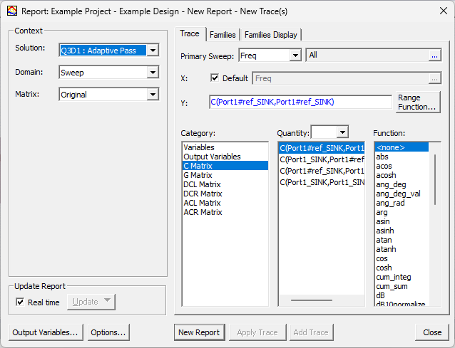
-
Navigate to the Families tab and select either all passes or an individual pass (if multiple sweeps are available) to view.
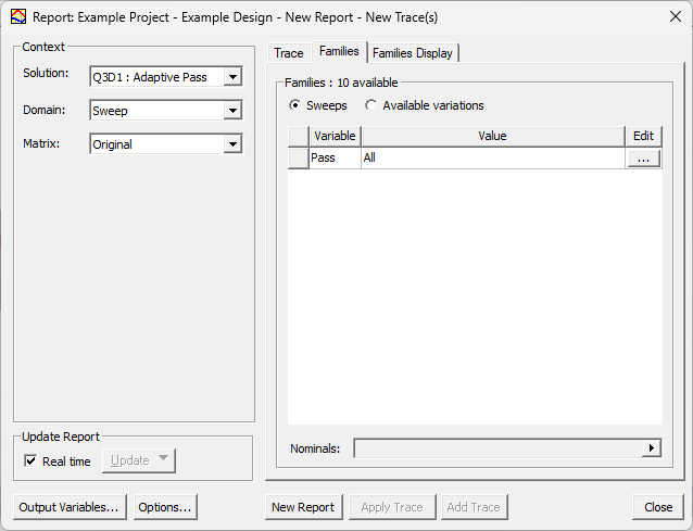
-
-
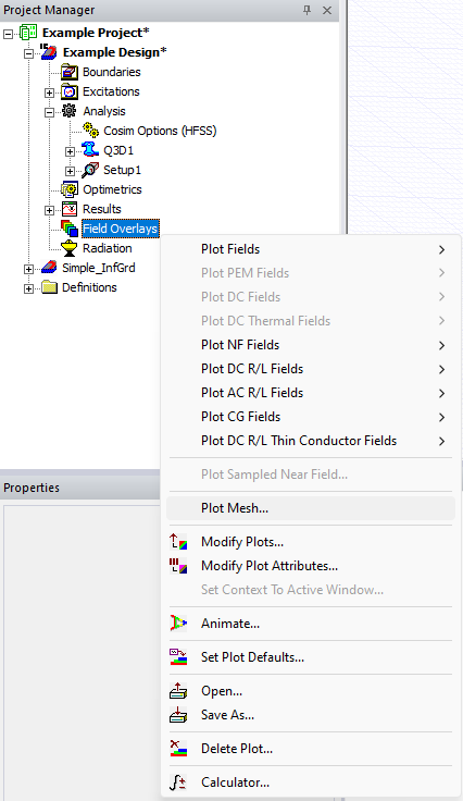
Navigate to the Project Manager window and right-click Field Overlays to view the available plot types. Several plot types are unique to Q3D solution setups (i.e., NF Fields, DC R/L Fields, AC R/L Fields, CG Fields, and DC R/L Thin Conductor Fields). Refer to Field Quantities.
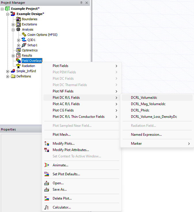
-
Select a plot type to open the Create Field Plot window.
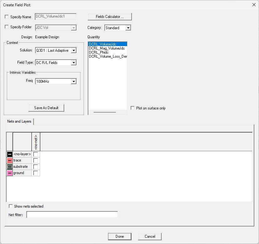
-
Make changes to the default settings, as appropriate. Then click Done to create the field plot. Refer to Plotting Field Overlays.
-
Navigate to the Project Manager window. Then right-click Field Overlays and select Plot Mesh to open the Create Mesh Plot window.
-
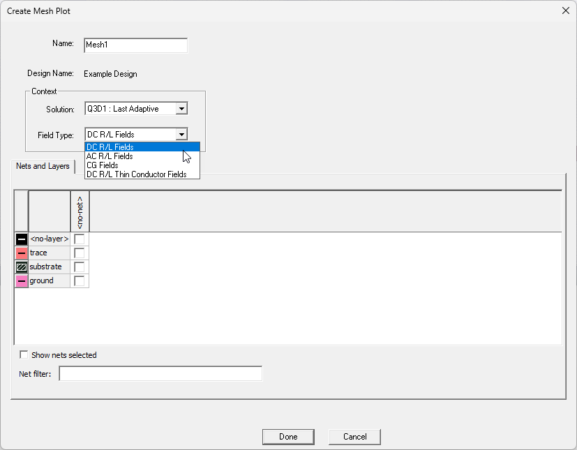
Select a Q3D solution from the Solution drop-down menu to populate the Field Type drop-down menu with options unique to Q3D solution setups (i.e., DC R/L Fields, AC R/L Fields, CG Fields, and DC R/L Thin Conductor Fields). Refer to Create Mesh Plot.
Changing Net Settings
Complete these steps to view all of the nets recognized by Q3D during simulation, and modify as appropriate.
-
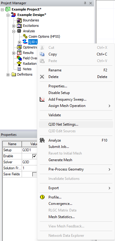
From the Project Manager window, expand Analysis. Then right-click the Q3D solution setup (e.g., Q3D1) and select Q3D Net Settings to open the Q3D Net Settings window.
-
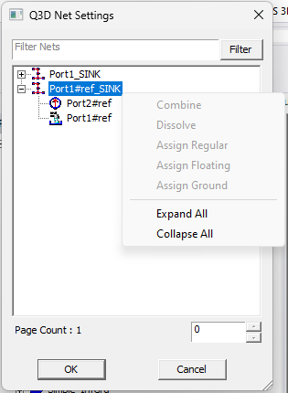
From the Q3D Net Settings window, right-click net groups that do not have terminal assignments and select Combine, Dissolve, Assign Regular, Assign Floating, or Assign Ground to add terminals.
-
Click OK to close the Q3D Net Settings window.
Editing Sources
Complete these steps to view and edit all of the design's sources.
-
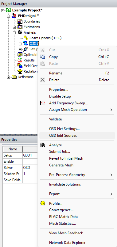
From the Project Manager window, expand Analysis. Then right-click the Q3D solution setup (e.g., Q3D1) and select Q3D Edit Sources to open the Edit Sources window.
-
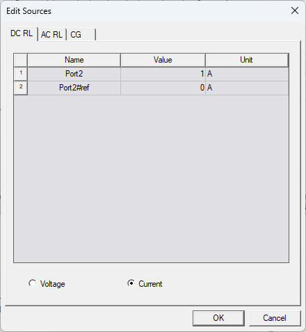
From the Edit Sources window, use the DC RL, AC RL, and CG tabs to edit the values and units of measurement for the design's ports. The available columns vary depending on source type. This feature allows greater flexibility in studying a larger set of excitation variations.
-
Click OK to close the Q3D Net Settings window.
Viewing RLGC Matrix Data
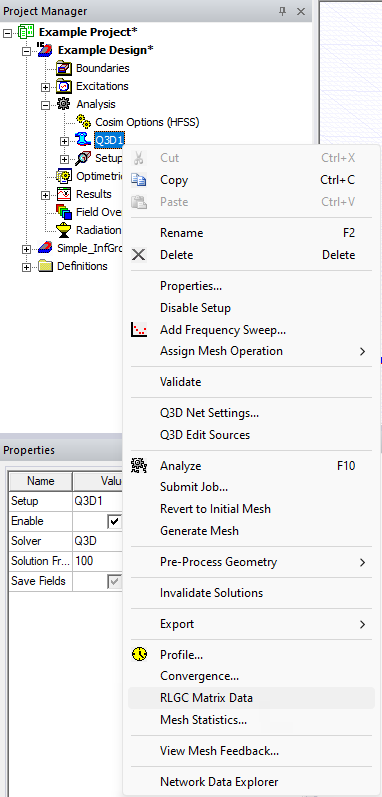
To view computed matrix data from a Q3D solution setup, navigate to the Project Manager window. Then right-click the Q3D solution setup (e.g., Q3D1) and select RLGC Matrix Data to open the Solution window. Refer to Viewing Matrix Data.
Exporting RLGC Data
Complete these steps to export RLGC matrix data or lumped RLGC data (i.e., Equivalent Circuit Export) from an analyzed solution.
-
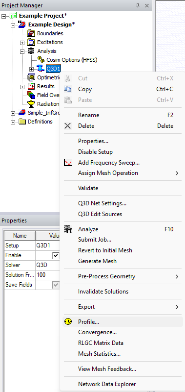
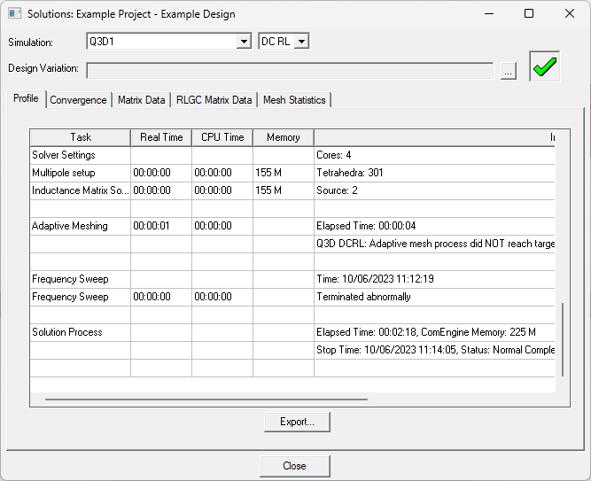
From the Project Manager window, expand Analysis. Then right-click the Q3D solution setup (e.g., Q3D1) and select Profile to open the Solutions window.
-
From the Solutions window, navigate to the RLGC Matrix Data tab.
-
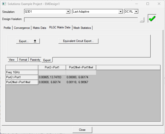
Select the Export subtab.
-
To export RLGC data in one of several file formats, or to export lumped RLGC data as an equivalent circuit file, complete steps in the following subsections.
Exporting RLGC Data in Several Formats
-
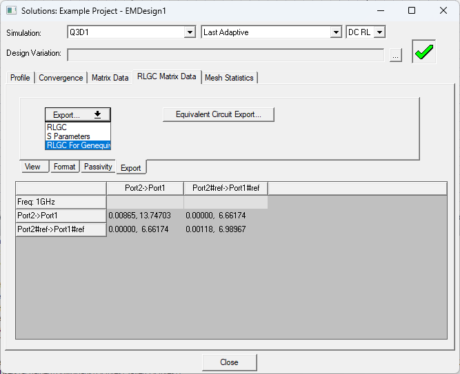
To export RLGC data, select a format from the Export drop-down menu.
 Note:
Note:Select RLGC For Genequiv to export a file with RLGC data ready for use by GenEquiv. The user can use a DOS command window to call GenEquiv and create a state space model.
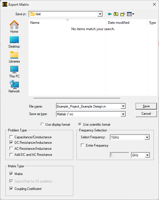
After making a selection from the drop-down menu, the Export Matrix window opens.
-
Enter a File name or accept the default name.
-
Select a file type from the Save as type drop-down menu (i.e., Matlab (*.m), Ansys EM Legacy Format Files (*.lvl), Comma Separated Value (*.csv), or Data Table(spreadsheet) (*.txt)).
-
From the Problem Type, Frequency Selection, and Matrix Type areas, choose the RLGC data to export.
-
Click Save to export the data and close the Export Matrix window.
Exporting Lumped RLGC Data in an Equivalent Circuit File Format
-
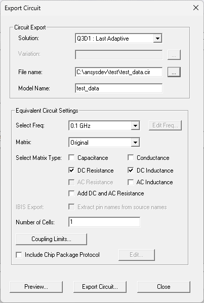
To export lumped RLGC data, click Equivalent Circuit Export to open the Export Circuit window.
-
From the Circuit Export area, specify the following:
-
Solution – use the drop-down menu to select the solution from which to export data (e.g., Q3D1 : Last Adaptive).
-
Variation – click ... to select a variation, if any are available.
- File Name – enter a file path and name for the circuit file to be exported (e.g., C:\ansysdev\test\test_data.cir) or click ... to open an explorer window, then navigate to an appropriate directory, enter a File name, and click Open.Important:
Circuit data can be exported in any of the following formats:
- Simplorer Netlist Files (*.sml)
- HSPICE Circuit (*.sp)
- IBIS Package Model (*.pkg)
- Maxwell Spice Circuit (*.spc)
- PSpice Circuit (*.lib)
- Spectre Circuit (*.ckt)
- Ansoft Designer Netlist (*.cir)
- Berkeley Spice Circuit (*.bsp)
- Cadence DML (*.dml)
- IBIS ICM (*.icm)
To export circuit data as an IBIS Package Model, use all lowercase names to facilitate portability between operating systems. The length should not be more than 20 characters.
To export circuit data in IBIS ICM format, use all lowercase names to facilitate portability between operating systems. The extension should be no more than three characters in length. There is no length restriction on the base file name; however, only lowercase letters, digits 0 through 9, underscore and hyphen are valid characters.
-
Model Name – enter a name for the model within the circuit file (e.g., test_data). Upper and lowercase letters, digits 0 through 9, and underscore are valid characters. Spaces are not accepted. Invalid characters will be replaced with underscores.
-
-
From the Equivalent Circuit Settings area, specify the following:
Select Freq – select a frequency from the drop-down menu (e.g., 0.1 GHz). For interpolating sweeps, click Edit Freq to open the Edit Sweep window, then enter Start and End values.
- Matrix – from the drop-down menu, select the Original solved matrix or a reduced matrices, if any are available.
- Select Matrix Type – check the check boxes adjacent to one or more matrix types for export (i.e., Capacitance, Conductance, DC Resistance, DC Inductance, AC Resistance, AC Inductance, and/or Add DC and AC Resistance).
- IBIS Export – by default, names are created in the form _NAME_src. Checking the Extract pin names from source names box will alter naming behavior so they are created as simply NAME.
- Number of Cells – enter the number of cells (i.e., sections) to be used while exporting the circuit. Finer discretization (i.e., a larger number of sections) gives a closer approximation to the underlying Partial Differential Equations. However, this also leads to increased simulation time. See the technical notes for Equivalent Circuits.
- Coupling Limits – click to open the Coupling Limits window.
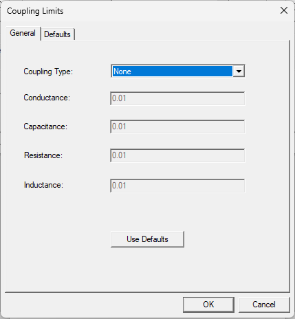
Select a Coupling Type, if appropriate (i.e., By Value or By Fraction of Self Term) and enter limit values in the Conductance, Capacitance, Resistance, and Inductance fields. RLCG values smaller than those specified will be ignored during export. Click OK to return to the Export Circuit window.
- Include Chip Package Protocol – check the box to activate Chip Package Protocol, then click Edit to open the Edit Chip Package Protocol window and specify header information for SPICE formats.
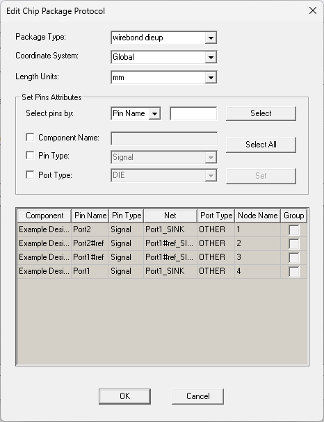
Chip Package Protocol (CPP) is a set of statements specifying the location, net information, and SPICE node name for each package pin (i.e., the landing pad of flip-chip bumps or the chip landing pad of bonding-wires). The CPP is embedded within a SPICE-compatible file header as comments and is primarily used to help automate the co-simulation of IC (i.e., die) and package or package/board (e.g., utilizing CPP to import the package or package and PCB model into the full chip dynamic voltage drop analysis, and the global IO-SSO analysis. Package/PCB simulation tool can utilize the CPP to import the chip model in the system level analysis). To utilize CPP, specify the following from the Edit Chip Package Protocolwindow:
- Package Type – select a Package Type from the drop-down menu (i.e., wirebond dieup, wirebond diedown, flipchip dieup, and flipchip diedown.
- Coordinate System – from the drop-down menu, select Global or a custom coordinate system, if any are available.
- Length Units – Select a unit of measurement from the drop-down menu (i.e., um, mm, or mil).
- From the Set Pins Attributes area, specify the following to select pins:
- Select pins by – select a sort attribute from the drop-down menu to sort pins by Component Name, Pin Name (i.e., number), Pin Type (i.e., signal or power ground), Net Name, or Port Type (i.e., DIE, PCB, VRM, or Other). Then enter a regular expression in the field and click Select to select the applicable pins.
- Select All – click to select all pins in the design.
- Check the Component Name, Pin Type, and Port Type boxes to modify the information for selected pin(s). Enter the Component Name in the field and/or select a Pin Type/Port Type from the drop-down menus.
- Click Set to apply changes.
Note:Checking the DC Resistance or DC Inductance boxes deactivates the boxes beside AC Resistance or AC Inductance, and vice versa. Check the Add DC and AC Resistance box if you want to create a circuit with a total resistance computed from AC and DC values.
-
Click OK to close the Edit Chip Package Protocol window.
-
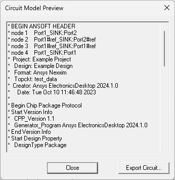
Click Preview to open the Circuit Model Preview window.
-
Click Close.
-
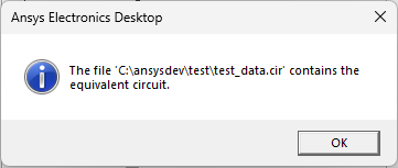
Click Export Circuit to complete the export. Once the export is finished, a message appears.
-
Click OK to close the message.
-
Click Close to exit the Export Circuit window.
Activating the Q3D Solution Setup Beta Feature
Complete these steps to enable the Q3D solution setup beta feature, then activate IC mode.
-
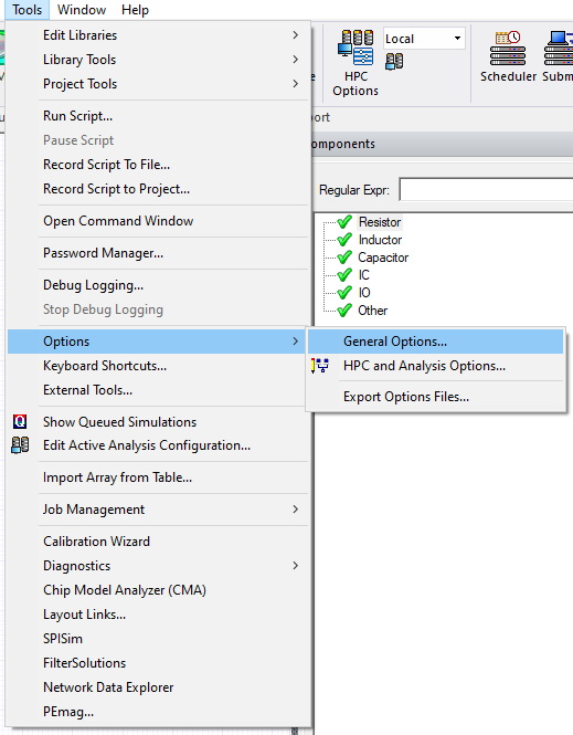
From the Tools menu, select Options > General Options to open the Options window
-
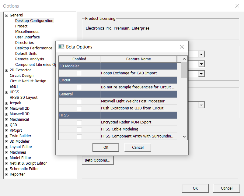
Expand General > Desktop Configuration and click Beta Options to open the Beta Options window
-
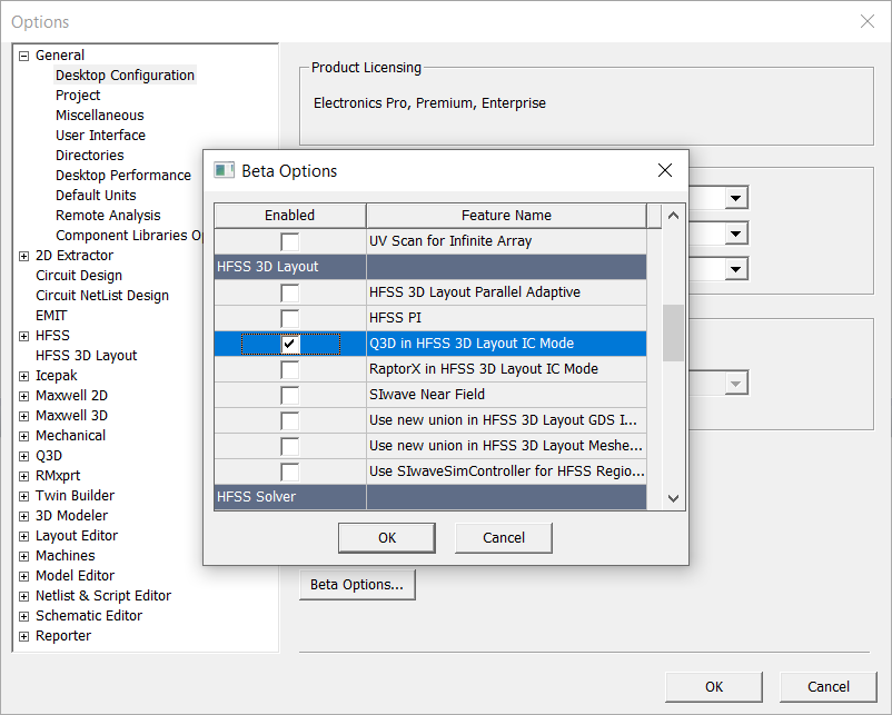
Scroll down and check the Q3D in HFSS 3D Layout IC Mode box.
-
Click OK to close the Beta Options window.
-
Click OK to close the Options window and open an Ansys Electronics Desktop prompt to restart the software. Users may be asked to save their work.

-
Click Yes to restart immediately.
-
After restarting the software, the Q3D solution setup is available from the locations described in the previous section.
The procedure is complete.
