VM277
VM277
Hall Plate in a Uniform Magnetic Field
Test Case
A series of static electromagnetic analyses is performed on a plate with length 2a, height 2b, and thickness c to determine the Hall voltage produced by a uniform magnetic field B perpendicular to the plate surfaces.
| Material Properties | Geometric Properties | Loading |
|---|---|---|
|
Hall constant Rh = -0.0001 m3/C Electrical resistivity = 1.6e-3 Ω*m Relative magnetic permeability µ = 1 |
a = 3e-3 m b = 3e-3 m c = 0.4e-3 m |
V0 = 3 V B = 0.8 T |
Analysis Assumptions and Modeling Notes
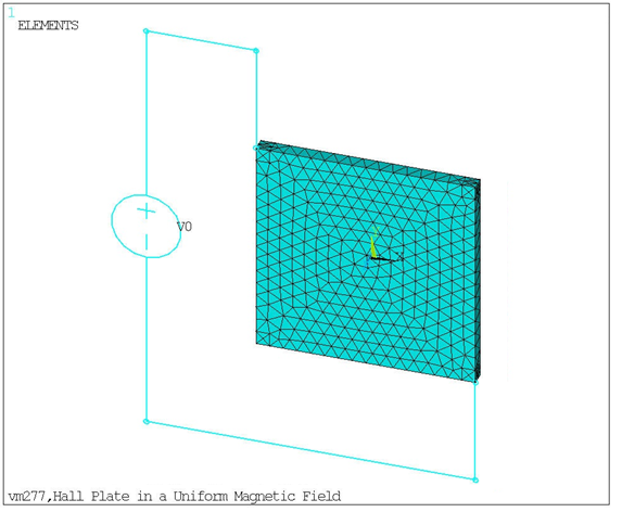
The initial electric potential distribution in the plate is created by a voltage V0 applied across a pair of contacts as shown in Figure 481: Hall Plate in a Uniform Magnetic Field Element Plot.
Electrical contacts are made by coupling the voltage of the nodes (CP, VOLT) located within a small volume at each corner of the Hall plate. The voltage load V0 was applied by coupling the voltage (CP, VOLT) of the independent voltage source (CIRCU124) (KEYOPT (1) = 4) with the corresponding electrical contacts on the plate. A ground is created by setting the voltage of one electrical contact to zero (D,,VOLT).
Meshing facet elements are used to depict the presence of wires.
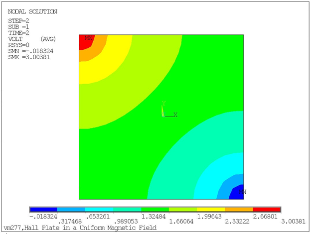
The first analysis is performed without any applied magnetic field to determine the offset voltage. The output voltage should be zero in the absence of a magnetic field; however, due to non-uniform meshing, the current distribution is not symmetrical, resulting in a small potential difference (offset voltage) across the output pair of contacts. In a real application, the offset voltage may be caused by various factors, such as mechanical stresses, material inhomogenities, or temperature variations.
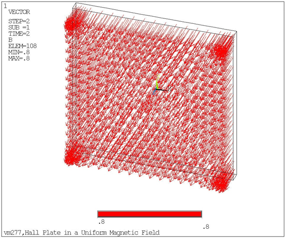
For the second static analysis, the output voltage is calculated when there is an applied magnetic field (B) perpendicular to the Hall plate (Figure 482: Vector Plot of Applied Magnetic Field on Hall Plate). The offset voltage is subtracted from this output voltage to determine the Hall voltage.
The target Hall voltage is obtained using Eq. 9.14 in the reference:

Where:
I = the current through the plate. This value is retrieved using *GET.