Link from Driven Modal or Terminal Antenna to SBR+ Design
HFSS lets you create a one-way link from a Driven Modal design or a Driven Terminal design with a single terminal to an SBR+ design. The source can be a finite array design, including designs with blockages. For finite array design, the phase center is configured using the physical cells, and automatically transformed to the virtual cells. The source design Excitations menu includes a Set Far Field Phase Center command that lets you specify the phase center for each lumped port and wave port it contains. You assign the phase center to a coordinate system. The far-field phase center determines the point from which SBR+ rays are launched when the linked source is configured as far-field. It has no effect for linked sources configured as near-field. It can affect the Export Element Pattern from Antenna Parameters dialog.
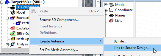
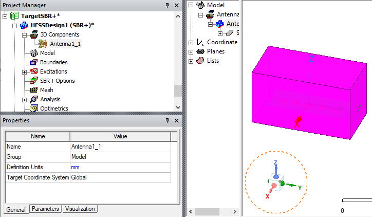
The target SBR+ design includes the associated command 3D Component>Create Antenna>Link to Source Design.
From the target design, you can select either Far-Field or Near-Field as the linked field style.
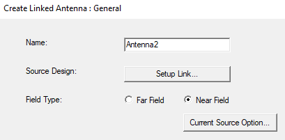
If you select Near Field, the Create Linked Antenna dialog includes a button for Current Source Option... allowing you to specify a customized power fraction. Use Global is the default. Enabling Thin Sources lets you specify a Power fraction should be greater than 0.1 and less than 1. Solutions are invalidated if you change current source conformance, use Thin Sources, Power Fraction, or change the Global option.
In the target design, the antenna link brings over the source design model and includes visualization options. The selected geometry is shown in its shaded view in the SBR+ target design with its designated color and transparency..
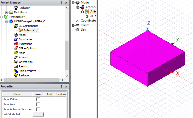
The linked source design appears in the target design under 3D Components. The source design ports appear in the target design under the excitation folder. You have the option when linking to a source project to Link as Composite Port, to simplify and speed up source projects with many excitations. However, you cannot edit those imported ports because they are part of the linked antenna component. You can turn on Field visualization of the source design by checking Show Pattern on the Visualization tab of the 3D component property in the target design.
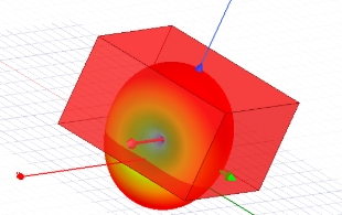
With Show Pattern checked, the source pattern is visible from the linked 3D Component bounding box in the target SBR+ design.
Prerequisites
- Set the phase center in the source design. The source design requires the presence of at least one wave port or lumped port to activate the Set Far-Field Phase Center... command.
- The source design must be solved before you can Show Pattern for the 3D Component Instance in the target SBR+ design.
- For simulation, the target design SBR+ solution frequency range must be in the range of source design.
- To support directivity and gain in the SBR+ design with the link, you must use an interpolating sweep with the 3D Fields Save Option selected in the linked design, either Save Fields (At Basis Freqs) or Save radiated fields only. This provides interpolatable S-parameters from the source design for the SBR+ target design.
- To model EM scattering effects of antennas in SBR+ simulations, you can select geometries from the source design to represent blockages. These can be model, or non-model objects. For this feature the SBR+ solver is passed a CAD representation of the antenna and it ignores this CAD representation when launching the rays from the antenna source but includes it when tracing the reflected rays from the platform.
Limitations
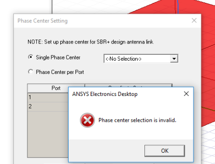
When the source design is in Composite-Driven Modal solution type or Composite-Driver Terminal with a single terminal:
- You can only choose one single phase center as the global phase center for all ports.
- Composite excitation becomes an incident wave in the target design. Therefore, we naturally should not have the port/mode option anymore.
- For Terminal designs, a single terminal is permitted.
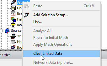
When you select Show Pattern, the pattern data is cached for future use. The cached data is available until the design is closed. If you update the source design, Clear Linked Data is available for you to clear the cached data. If you clear the Linked data, field pattern is re-computed when you select Show Pattern again.
To model blockage structures, the source design can be Driven Modal or Driven terminal or a finite array. If you use a finite array, the Model Blockage tab on the Setup Link dialog shows up if the array has model / non-model blockage objects. The GUI operations for array blockages are same as non-array projects. See steps 4 to 7 below.
Creating a Link from Driven Modal or Driven Terminal Source to SBR+ Target
To create a link from a Driven Model Source or Driven Terminal Source to an SBR+ target:
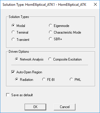
- Set up a driven Modal solution or Driven Terminal as the source.
You can choose any Modal options, although if you choose Composite Excitation, you must choose a single phase center for all ports. You can use Auto-Assign Region options if convenient.
All ports in the source design must be either wave ports or lump ports.
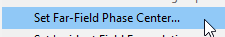
- Set the Phase Center in the Source design. The phase center(s) determine the point(s) from which SBR+ rays are launched when the linked source is configured as far-field. It is important for accurate results to position the phase center as near as possible to the physical phase center of the antenna for the selected port, especially if the source is placed nearby to SBR+ scattering structures. Otherwise, the accuracy of ray fields illuminating nearby structures will be compromised, leading to inaccurate scattered fields and final results. Either right-click Excitations in the Project tree and select Set Far Field Phase Center... or click HFSS>Excitations>Set Far Field Phase Center...
The Phase Center Setting dialog appears, with Phase Center per Port selected as default with the mode <- Port Location->. By using Phase center per Port, you have more fine-grained control over each phase center. This feature provides a convenient option to assign phase center at port location (port geometrical center), which is a common selection for Phase Center per Port mode. If you have created additional Coordinate Systems, these appear in the drop-down menu as options for the phase center.
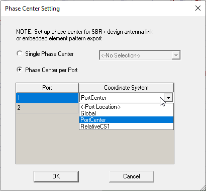
Single Phase Center is to assign the global option to all the ports (one port or multiple ports with the same phase center option). You also have the option to select Link as Composite Port when you setup up the link from HFSS to SBR+ design. Phase Center Per Port lets you specify different phase centers for different ports. Validation checks to ensure that each port is assigned a valid phase center. You must not leave any ports with <No Selection>.
In the case of a design using the Beta feature for subarrays, the Phase Reference Setting dialog shows composite groups if you want to specify unique phase reference for each group. In this case, the “Port Location” selection is not available, and you must select an actual reference coordinate system.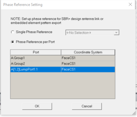
- When you have completed the source design setting (phase centers, solve setups, etc) and solved it, create an SBR+ design as the target design.
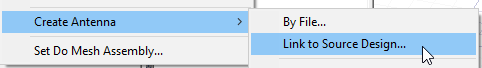
- Right-click 3D Components in the Project tree and select Create Antenna>Link to Source Design...
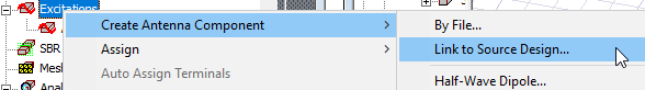
You can also right-click Excitations in the Project tree to select Create Antenna>Link to Source Design...
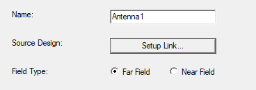
The Create Linked Antenna dialog appears.
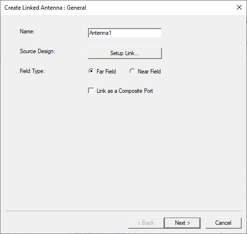
Select Far Field or Near Field as appropriate.
The Link as Composite Port option addresses the situation where an imported design contains many ports. By default, the model window displays the same number of virtual ports in the SBR+ target design. However, if the source design contains many virtual ports, they will look cluttered and require significant computational resources to solve. You create a single composite port in the SBR+ target design to represent all the ports in the HFSS source design. During computation, the SBR+ target design sends the information about a single composite port to the solver, rather than information about all the ports. This saves a significant amount of resources. For further discussion, see Link as Composite Port.
- Click Setup Link...
The Setup Link dialog appears.
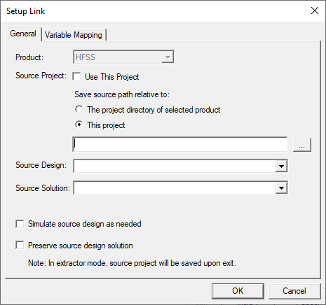
If the source design is in a different project, you can click the ellipsis button [...] to open a file browser to select the project of interest. When you select the project and OK the browser, the fields are filled in.
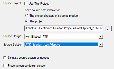
If the source design is in the same project, you can check Use this Project and select from available Source Designs.
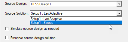
If you have defined an interpolating frequency sweep in the source design, you can select it on the drop-down for the source solution. (This feature supports directivity and gain in the SBR+ design with the link. (See Requirements for Creating a Gain Report for SBR+ Design with Driven Modal or Terminal Source). It provides the S-Parametersfrom the source to the target. In the source sweep setup, you must have selected a 3D Fields Save Option.)
For this release Model blockages can handled as a separate step outside creation of the linked design, by selecting geometry from the SBR+ region to be designated as “Model Blockage” associated with a particular source antenna, as described in . Note there is no longer any restriction on what objects and/or materials can be designated as “model blockage” geometry. For either solution type, SBR+ or hybrid HFSS-SBR+, this selection is from the available SBR+ region geometry objects. Once you specify antenna blockage geometries for each source antenna, we can then solve the combined target SBR+ design. For details see Design Flow for SBR+ Solution Type.
If you use the older method for designating blockages, once you select the source design, additional tabs for Model Blockage (if model or non-model blockages exist in the source) and Model Visualization appear.
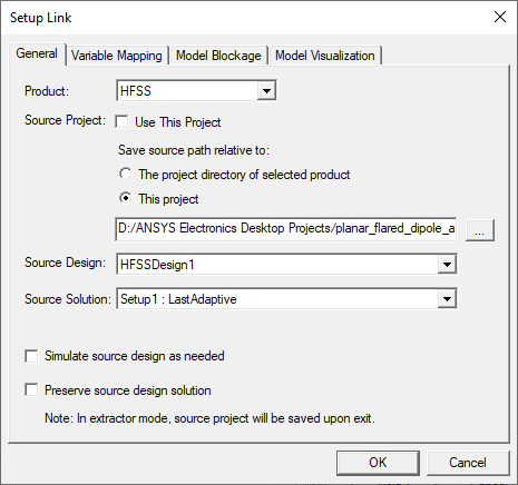
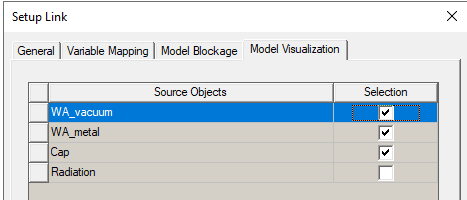
The Visualization tab lets you specify how the linked model is displayed in the SBR+ target design.
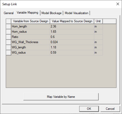
- The Variable Mapping tab lists variables and lets you define mappings between the driven modal source design and the SBR+ target design, if necessary.
- The Model Blockage tab lets you select geometries from source design to represent the blockage structure. Non-solve inside, and non-model objects are available for selection.
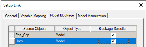
For Non-model objects, you can select <Not Include> Perfect Conductor, or Perfect Absorber.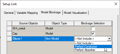
In many cases, it is sufficient to represent SBR+ sources entirely in terms of their far-field or near-field radiation characteristics, and there is no need to configure Model Blockage. However, in some cases, the antenna structure can generate significant secondary scattering after rays have first reflected off the main scattering geometry that the source illuminates. An example would be a feed antenna blocking part of the main beam of a reflector antenna, where the reflector surface is simulated using SBR+. Model and non-model structures selected under Blockage Selection will have special behavior relative to SBR+ ray-tracing. These surfaces will be invisible to SBR+ rays when they are first launched from the source. However, after the first bounce, they will interact with SBR+ rays just like any other surfaces in the scattering geometry (with some further qualification, described shortly). For example, to capture reduced reflector antenna gain due to blockage by the feed horn, you may select the elements representing the body of the horn under Blockage Selection. In some cases, the antenna structure may be too detailed to effectively interact with SBR+ rays, recognizing that ray-tracing is a high-frequency (short wavelength) approximation. In those situations, one may instead create a simplified blocking structure, such as a rectangular or circular plate, to stand in for the physical antenna structure. To do this, create the simplified blocking structure as one or more non-model objects in the source design and then select them under Blockage Selection, configuring them as either Perfect Conductor or Perfect Absorber.
The behavior of model and non-model objects selected under Blockage Selection have some further qualifications in the context of SBR+ with multiple source antennas. Suppose there are two antennas A and B, and both have Model Blockage objects selected, designated as SA and SB, respectively. S_A will be invisible to first-bounce SBR+ rays launched from antenna A, and then become visible on subsequent bounces. However, SB will always be visible to SBR+ rays launched from antenna A, even on the first bounce. A related point is that when rays hit S_A, they will generate scattered fields to every antenna accept to antenna A. Likewise, when rays hit SB, they generate scattered fields to every antenna accept to antenna B. - The Visualization tab lets you specify how the linked model is displayed in the SBR+ target design.
For example: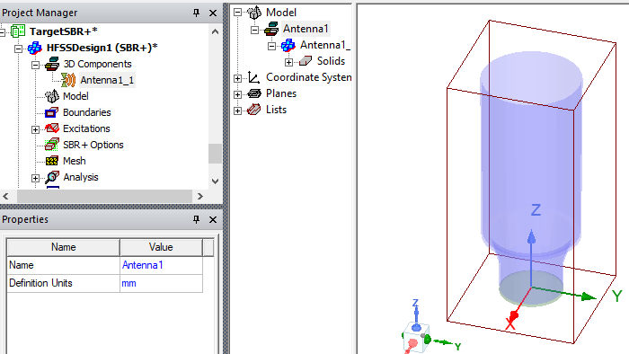
Selecting the linked 3D Component also provides a Visualization tab in the properties with additional control over how a linked project displays in the SBR+ target design.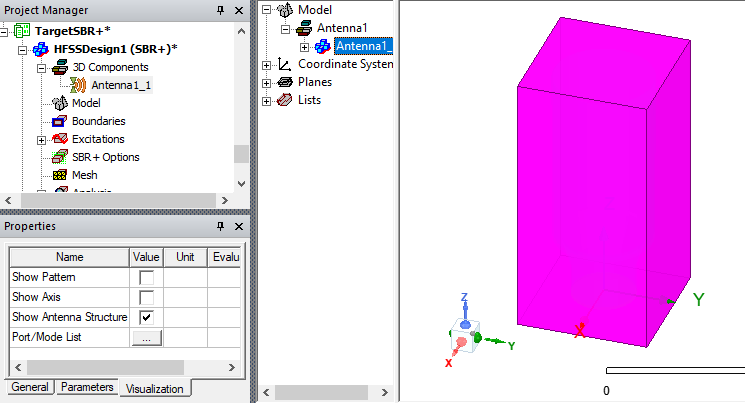
You can also gain access to the Setup Link Visualization tab by Editing the definition of the 3D Component.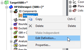
This opens the Setup Link: General window, where you can click the Setup Link... button. - Click OK to finish importing a linked antenna to the target SBR+ Design. The target design displays the linked antenna as a 3D Model in the Project tree and in the Model window as a model based on how you specify the visualization.
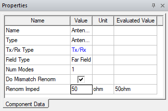
- Ports appear in the Project tree under Excitations. If you right click on the Excitations icon, you can view and edit Tx/Rx selection for all fields, including coupling between ports within the same antenna and self coupling. The properties for each excitation shows the current Tx/Rx type. If you select do Mismatch Renorm, an editable Renorm Imped property appears which lets you Renormalize linked ports.
- Select the 3D Component for the source antenna in the target Project tree to view the properties.
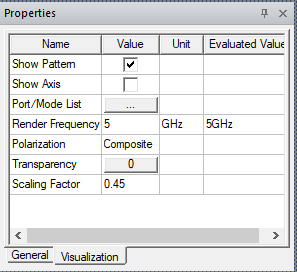
If you select the Visualization tab, you see the following properties.
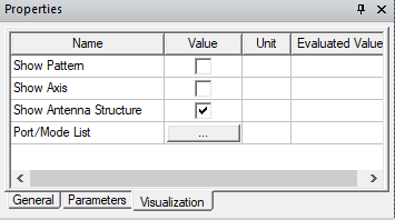
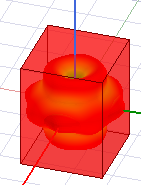
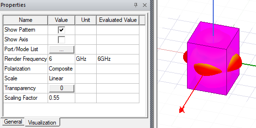
If you have previously solved the source design, and correctly assigned valid phase centers, you can check Show Pattern, and see additional display properties. The antenna pattern is computed and displayed in the bounding box in the Model window.
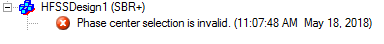
If the source design has not been solved, the Message window will display an error message.
If you update the source design, the Clear Linked Data command becomes available for you to clear the cached data.
If you clear the linked data, the field pattern is re-computed when you check Show Pattern again.
If you made changes to the source design that conflict with the link or phase center configuration, an error message is displayed.
If you check the Show Axis property, the phase center axis is shown at the antenna pattern.
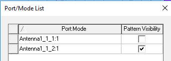
The Port/Mode List is available unless the source design is driven modal composite. If you click the ellipsis [...] button for Port/Mode List on the Visualization tab properties, a dialog displays that lets you select which ports to show:
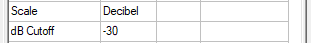
The Scale property can be Decible, Linear, or Power.
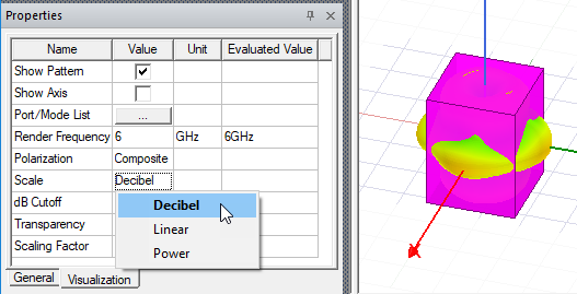
If you select Decibel, an additional property for dB Cutoff appears.
Simulation Setup for Driven Modal Antenna to SBR+ Design Link
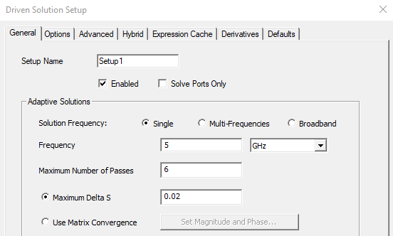
Once you have configured the SBR+ design with an Linked Antenna, you set up a model object and Solution Setup. The simulation frequencies in target design must fall in the range of the source design frequencies. Below is an example of source design setting and target design setting, using compatible frequencies. and Save Far fields so that Gain can be plotted.
Example Source Design Setup
Source Design Frequency Sweep
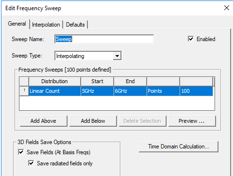
The sweep will be selectable in the Source link, and the 3D Fields Save Options permit the Target SRB+ design to compute far fields and plot gain.
Example Target Design Solution Setup
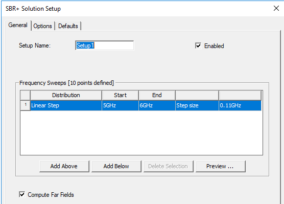
Compute Far fields is so that a Gain Report can be plotted based on the fields saved from an interpolating sweep in the linked source design..
Viewing Results in the SBR+ Simulation
After you run an SBR+ simulation with linked Model antenna, you can create a variety of reports, including S Parameters, Far Fields, Gain, and Antenna Parameters. 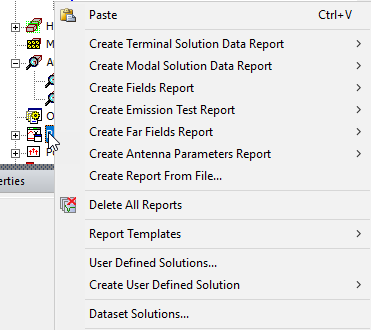
You must create a Far Field Setup to access the Far Fields and Antenna Parameters reports.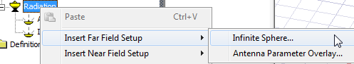
When a driven modal or driven terminal antenna is linked to an SBR+ target, an additional SBR+ power loss is considered for radiated power calculation. See Technical Notes: Radiated Power.
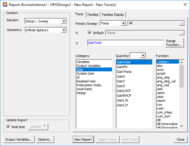
Requirements for Creating a Gain Report for SBR+ Design with Driven Modal or Terminal Source
If you have created an Infinite Sphere, solved an Interpolating Frequency sweep in the Source design and saved the 3D fields, and selected Compute Far Fields in the Source setup, you can create a Gain Report.