
Using the Layer Stackup Wizard
The Layer Stackup Wizard is a powerful utility that allows users to build and modify laminate layer stacks to meet precise impedance requirements for single-ended and differential microstrips and striplines. SIwave’s fast and accurate Method of Moments transmission line solver is used in all calculations and fully accounts for frequency-dependent dielectrics, non-uniform (e.g., trapezoidal) trace cross-sections, and surface roughness parameters. In Analysis mode, users can assess the impact of changing material parameters, layer thicknesses, etc., on the impedance of single-ended and differential lines whose width and separation are fixed. In Synthesis mode, users can compute trace width required to achieve a specified impedance value on a given layer. For differential nets, users can compute either trace width or trace separation to achieve a given impedance and trace separation (or width) values. Computed trace widths can then be applied to SIwave’s layout editor. Traces that are subsequently routed on layers with updated width values will have the exact impedance value specified in the Stackup Wizard.
A key component of this utility is the interactive, 3D visualization of the layer stack. This view, which can be panned, zoomed, and rotated using the mouse, provides an intuitive understanding of the dimensions and composition of the layer stack.
Complete these steps to use the Layer Stackup Wizard.
- Click Home > Layer Stackup Wizard. to open the Layer Stackup Wizard window.
- Control Pane – located on the left, this pane allows you to configure the layer stack, and to calculate impedance, differential impedance, and trace width/pitch.
- View Pane – located on the right, this pane displays the current layer stack. The pane automatically updates as you change settings in the Control Pane, and you can add, remove, or edit certain layer properties directly from this pane. Use the mouse or hot keys to rotate and zoom the model. Use Ctrl+D to auto-zoom.

The window contains two panes:
To configure the layer stackup from the Control Pane:
- From the 3D View Controls area, select your appropriate options:
- Ignore layer thickness – checking this renders all layers at the same thickness. If this option is unchecked, layers display at their actual thicknesses.
- Show layer name – checking this displays layer names. If this option is unchecked, layer material names display instead.
- Set conformal coat – select this check box to add conformal coat layers. These layers are a set of dielectric
layers on the top and bottom of all packages and PCBs in the design.
They have a default material of "SolderMask" and a default thickness
of 15 microns. They are shown with a Layer Type of "CONFORMAL_COAT".
Note:
If dielectric layers are already present above the top layer and below the bottom layer, their material is changed to SolderMask and the layer type is changed to Conformal Coat.
- Units – use this drop-down menu to update the units displayed in the View Pane, as well as in the impedance calculator.
- Enable Dynamic Update – when enabled, dynamic update performs the following actions when any change is made in the Layer Stackup window:
- The design updates.
- Impedance and differential impedance are recalculated.
- W-element plots are recalculated and replotted.
- Layer spacing – use the slider to increase or decrease the space between layers.
- Font size – use the slider to increase or decrease the size of the font in the View Pane.
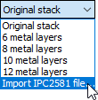
- Stack Configuration – use the drop-down menu to select Original Stack, or select a specific number of metal layers for display. You can also import an IPC2581 file.
- Selected Layer Name – displays the name of the currently selected layer. Select layers from the View Pane.
- Trace Cross Section – displays the shape of the current trace cross section, if any. Clicking this opens the Trace Cross Section Shape Editor. See: Modifying the Cross Section of Traces.
- Frequency – drop-down menu that allows you to select a frequency.
- Reset View – click to reset the View Pane to its default view.
- Export IPC2581 File – prompts you to select an *.xml or *.cvg file for export.
- Export W-Element – allows you to export the w-element.
- Use width/pitch in W-element – uses the calculated trace width or pitch in the w-element analysis.
- Project Variables – opens a window that allows you to define project variables for w-element export.
To configure the layer stackup from the View Pane:
- Double-click any layer to open its Layer Properties window.

From here, you can change the layer's Thickness and Material.
- Right-click a layer in the View Pane to view additional options:

You can insert signal or dielectric layers, or remove the selected layer.
You can also right-click any layer and click Show Impedance Plots to open the plots in a new window:

This plot is modeless. Make any change in the Layer Stackup Wizard to enable the Update button. For more information about plots in SIwave, see Changing Plot Display Options and Additional Plotting Actions.
From the Layer Stackup Wizard, you can also: