Enabling Solver Options in Encrypted Layers
Complete these steps to enable solver options and surface roughness in an encrypted stackup.
-
To open the Edit Layers window, do one of the following from the Layout tab.
-
From the Layout ribbon, select
 Layers dialog.
 -
From the Layout or Footprint menu, select Layers .
-
Right-click in the Layout Editor and select Edit Layers.
-
From the Grid Control Table, check any/all of the active boxes in the Solver column, or select one or more layers and check the Solver box in the Analysis area.

-
By default, layers do not have surface roughness. If appropriate, add Rough status to one or more signal layers by selecting the layer(s) and checking the Rough box in the Analysis area. The roughness is added to the layer when its mesh is created. Refer to Setting the Layer Surface Roughness.

-
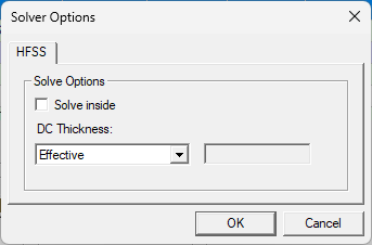
Checking either Solver boxes in the Grid Control Table or the Solver box in the Analysis area activates the Solver button. Click Solver to open the Solver Options window.

-
From the Solver Options window, do the following:
-
Solve inside check box — check to enable all objects in the layer to have the "solver inside" attribute . It is possible to perform solve inside on an object-by-object basis. Refer to HFSS 3D Layout Properties
-
DC Thickness drop-down menu — controls how DC thickness is calculated for the conductor lumps on the layer:
- Effective — calculates thickness as twice the volume/surface area.
- Layer — uses the layer's thickness.
- Manual — enter a value in the field.
-
