VM294
VM294
Fourier Series Analysis of a Diode Rectified Circuit
Test Case
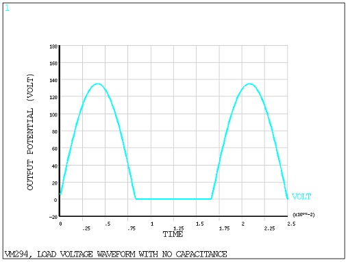
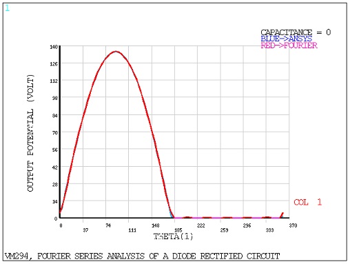
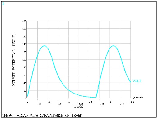
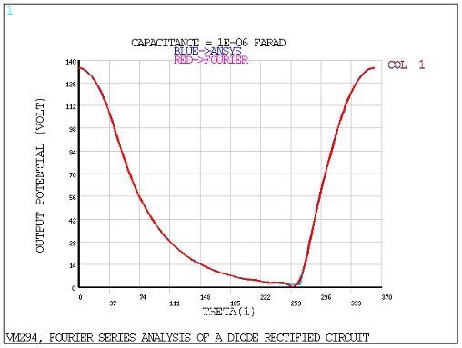
Compute the Fourier series coefficients of the output voltages for three configurations of
the following circuit: first with no capacity, as shown in Problem Sketch 1 in Figure 513: Diode Rectified Circuit Problem Sketch; second, with a capacitor C(2) of value 1 x
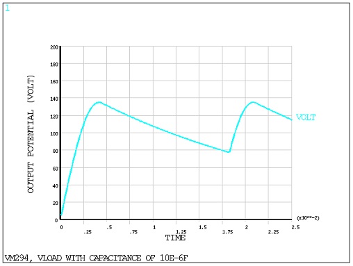
10-6 Farads, as shown in Problem Sketch 2; and third with a
capacitor C(3) of value 10 x 10-6 Farads, as shown in Problem
Sketch 2. In all three cases, the circuit is driven with a 60 Hz, 125 V AC power source and
contains a 2500  resistor and an ideal diode as indicated.

| Material Properties | Loading | |||
|---|---|---|---|---|
|
 V V |
Analysis Assumptions and Modeling Notes
The diode is modeled with CIRCU125 elements, configured to behave as an ideal diode with zero forward resistance, infinite backward resistance, and a zero forward voltage threshold. The voltage source, resistor, and capacitor are modeled with CIRCU124 elements, the three different behaviors being achieved with different KEYOPT settings.
For each of the three circuits, Mechanical APDL is used to calculate the Fourier series
coefficients,  ,
,  , and
, and  in the following equation:

where  is the period.
Calculatuon of the coefficients for the two circuits with the capacitor is significantly more involved than the first case without the capacitor.