
Component Information

This information will generally describe the component. The Component Name is used in the schematic or in the SML file name to identify the component for later use.
When naming the component, spaces are not valid characters. Using a space in the component name will result in an error. The valid characters for the component name are a-z, A-Z, 0-9, and _.
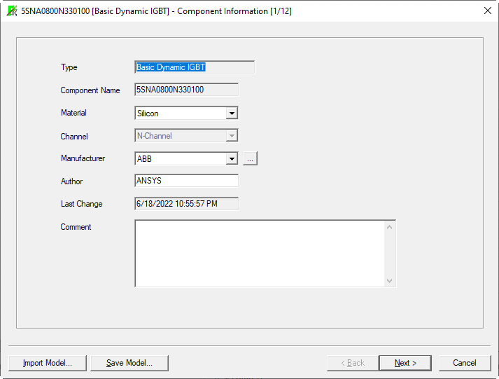
- Enter the information in the fields to identify the component.
-
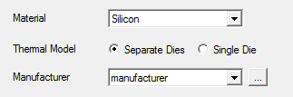
The selection of the material is used to account for major behavioral differences between devices made from different materials. Currently Si and SiC for wide bandgap devices are supported. The compensation for the different values Vgap is done internally through appropriate adjustments of the correction coefficients.
-
During the definition of a new device, the channel type (N-type or P-type) can be selected. For P-channel devices all values for any characteristic on following pages still must be entered as positive values. The fitting process will account for the actual sign of the value.
- The selection of the thermal model is available for Power MOSFET models. Some MOSFETs use a common die for the FET and the freewheeling diode. This selection is used to specify the type of the die. If the device has a single die for the FET and the FWD, the page for the thermal model of the FWD is not used. All parameters for the thermal behavior of the device are taken from the page for the thermal parameters of the FET.
- To define the Switching Energy and Delay
Time Measurement criteria for a Basic Dynamic or Advanced Dynamic
IGBT or a Basic Dynamic Power MOSFET, click
 next to the Manufacturer field
to open the Manufacturer
Data dialog box in which you can set the start and stop times
for Eon, t(on),
Eoff, and t(off)
for the named manufacturer.
Note:
next to the Manufacturer field
to open the Manufacturer
Data dialog box in which you can set the start and stop times
for Eon, t(on),
Eoff, and t(off)
for the named manufacturer.
Note:These criteria are not enabled for Average IGBT and Average Power MOSFET device characterization.
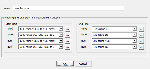
Use the Manufacturer
Data dialog box to select the start and stop criteria
for the switching times and energies from predefined lists. Because each
manufacturer uses different criteria for these parameters, it is important
to select the criteria which match the manufacturer of the device being
characterized to help ensure that the configured device converges to
the desired characteristics. Some choices are not yet available in the
characterization tool. In such cases an approximation must be made. In
most cases, the off-time starts when VGE starts
to drop to when IC has dropped sufficiently; the on-time starts when VGE starts to increase to when IC has sufficiently
increased. Click to display a dialog box with image buttons that depict each of the possible selections. Select the image that best matches the criteria and the combo box will be updated.
Some data sheets provide separate information for td(on/off), tr, and tf. The characterization process is not capable of fitting for td(on/off), tr, or tf separately. Therefore, it is fitting for the complete On-switch or Off-switch times, which consist of td(on) + tr = t(on) for the On-switch time and td(off) + tf = t(off) for the Off-switch time.
The following procedures suggest approximations for several manufacturers. If you have questions about these approximations, contact Ansys support.
|
Vendor |
Guidelines |
|
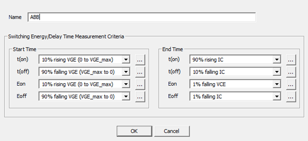
ABB |
ABB defines its switching criteria in its Applying IGBTs Application Note on its website. Ansys suggests the following on-time settings:
Ansys suggests the following off-time settings:
The on-switching energy loss, Eon, is measured as starting at 10% after zero-crossing of rising VGE and stopping at 10 to 20 microseconds beyond this point. The off-switching energy loss, Eoff, is defined as starting at 90% of falling VGE and stopping at stopping at 10 to 20 microseconds beyond this point. Due to limitations of the device characterization tool, the following settings provide an approximation of these energy parameters: Ansys suggests the following on-switch energy settings:
Ansys suggests the following off-switch energy settings:
|
|
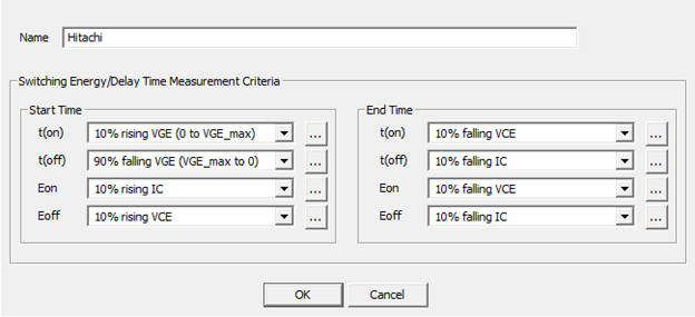
Hitachi |
Hitachi defines its switching criteria in its datasheets. Ansys suggests the following on-time settings:
Ansys suggests the following off-time settings:
Ansys suggests the following on-switch energy settings:
Ansys suggests the following off-switch energy settings:
|
|
Infineon/Eupec |
Infineon has defined its switching criteria for the switching times in the Infineon application note AN2011-05, Figure 22. Ansys suggests the following on-time settings:
Ansys suggests the following off-time settings:
Ansys suggests the following on-switch energy settings:
Ansys suggests the following off-switch energy settings:
Note: Older application notes (for example, AN2007-4, Figure 43) described the measurement for the On-switch time and Off-switch time with a time gap between the end of the delay time td(on) or td(off) and the beginning of the rise time tr or the fall time tf. This older measurement definition is no longer supported.
|
|
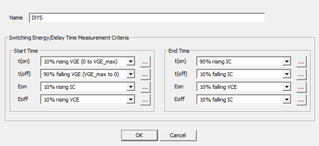
IXYS |
IXYS has defined its switching criteria for the switching times in its IGBT application note IXAN0063. Ansys suggests the following on-time settings:
Ansys suggests the following off-time settings:
Ansys suggests the following on-switch energy settings:
Ansys suggests the following off-switch energy settings:
|
|
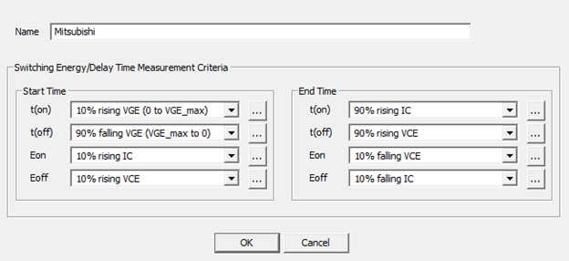
Mitsubishi |
Mitsubishi uses varying definitions for its switching criteria. The datasheets usually supply the definitions that were used. Regrettably, many datasheets do not supply the values of Eon and Eoff, so it will not be possible to fit for these characteristics. Consequently, you need not fit for these values in the Dynamic Model Input section. Ansys suggests the following on-time settings:
Ansys suggests the following off-time settings:
Ansys suggests the following on-switch energy settings:
Ansys suggests the following off-switch energy settings:
|
|
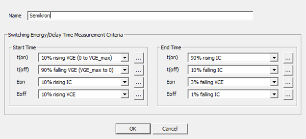
Semikron |
Semikron defines its switching criteria in its Technical Applications datasheet on its website. Ansys suggests the following on-time settings:
Ansys suggests the following off-time settings:
Ansys suggests the following on-switch energy settings:
Ansys suggests the following off-switch energy settings:
|
|
Fuji |
Fuji has defined its switching criteria for the switching times in its IGBT Application notes (REH983). Many datasheets do not supply the values of Eon and Eoff, so it will not be possible to fit for these characteristics. You then need to not fit for these values in the Dynamic Model Input section. The on-time is defined as the time from the input signal rising above the threshold voltage to 90% of rising Ic. The starting time is not yet available in the wizard. Ansys suggests starting at 10% of rising VGE and stopping at 90% of Ic. This time is found in the data-sheet as toff. The off-time is defined as starting when the input signal drops below the threshold voltage and stops at 10% of falling Ic. The starting time is not yet available in the wizard. Ansys suggests starting at 90% of VGE and stopping at 10% of Ic. This time can be found in the data-sheet as toff. Fuji regularly does not supply the switching losses Eon and Eoff. Nor do there appear to be definitions for the losses in the application notes. A probable good approximation is to start Eon at 10% of rising VGE and stop at 1% of falling VCE. A probable good approximation is to start Eon at 90% of falling VGE and stopping at 1% of falling Ic. |
- Click Next to continue characterizing the device (See Nominal Working Point Values).