Dynamic Model Input (Basic and Advanced Dynamic IGBT and Basic Dynamic Power MOSFET)

In the Dynamic Model Input page, you can enter the data for the calculation of the energy correction coefficients and switching delay times for the Basic and Advanced Dynamic IGBT and the Basic Dynamic Power MOSFET models. The switching energy data under at least six different working conditions are required to calculate the complete set of energy correction coefficients.
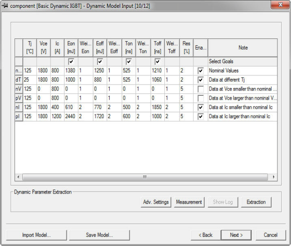
These six data sets must be entered following a predefined format:
- The first row is the set of data under the nominal working conditions.
- Each subsequent row may have only one change in the working condition; for example, temperature T is different from the value in the nominal values row. The required variation for each row is listed in the Note column.
If any of these data sets are not available, clear the Enable check box for the row and the corresponding coefficients will remain at their default values (see the IGBT Basic Dynamic model reference in the component help for more information on the algorithm of the switching energy calculation). Additional information provided will be used to fine tune these coefficients.
Dynamic model parameters of the Basic Dynamic IGBT model
|
Eon |
Turn-On Switching Loss |
|
Eoff |
Turn-Off Switching Loss |
|
Ton |
Turn-On Time (vendor-specific) |
|
Toff |
Turn-Off Time (vendor-specific) |
|
Residue |
The target error in the parameter fitting for the specified case. In general, lowering the residue results in higher accuracy at the expense of extraction time; however, lower residues are not always achievable. Increasing the residue values increases the probability of successful convergence. The default provides good model accuracy with reasonable extraction time. Fitting of the nominal working point must converge before the extraction process can proceed to other working points. Failure to converge on any other working point will warn you of the failure and provide you with the option to continue the extraction process with other working points. Change the residue to place more or less emphasis on fitting to a set of parameters. |
In addition to those dynamic parameters, the following table lists the parameters whose values can be determined without the need of a measuring template. These values result from either integration or direct measurement of the simulated wave form.
|
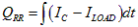
Qrr |
Reverse recovery charge |
|
Irr |
Reverse recovery absolute current peak |
You can adjust weights for the switching energies, Eon and Eoff, the delay times, Ton and Toff, and for the reverse recovery characteristics, Qrr and Irr. A higher Weight gives a higher importance to fit more precisely to that particular value. A default weight of 1 is set for these parameters. By default, the reverse recovery characteristics are not used. They can be turned on the Model & Goal Settings page in the Advanced Settings dialog box.
It is possible to define the Switching Energy and Delay Time Measurement criteria; click Measurementto open the Measurement Data dialog box in which you can set the start and stop times for Eon, t(on), Eoff, and t(off) for the device being characterized.
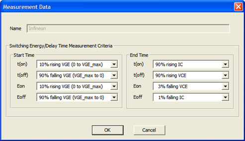
The Measurement Data dialog box contains the same settings as those in the Manufacturer Data dialog box (see Component Information).
When finished, click Next to continue characterizing the device (see Dynamic Parameter Validation).
Dynamic Parameters of the Advanced Dynamic IGBT Model
The first group of parameters is the same as those used for the Basic Dynamic IGBT model.
|
Eon |
Turn-On Switching Loss |
|
Eoff |
Turn-Off Switching Loss |
|
Ton |
Turn-On Time (vendor-specific) |
|
Toff |
Turn-Off Time (vendor-specific) |
In addition to the basic dynamic parameters, the following table lists the advanced dynamic parameters whose values can be determined without the need of a template function fitting. These values result from either integration or interpolation of the simulated wave form.
|
Qrr |
Reverse recovery charge |
|
Flux |
Off switch voltage overshoot area |
|
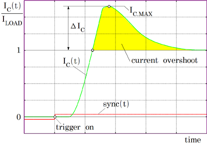
Cos |
Relative current overshoot at on switch |
|
Vos |
Relative voltage overshoot at off switch |
|
TdG |
Input voltage delay time before current rise |
|
TrG |
Input voltage rise time |
|
TsG |
Input voltage storage time before current fall |
|
TfG |
Input voltage fall time |
|
TdI |
Load current delay time before current rise |
|
TrI |
Load current rise time |
|
TsI |
Load current storage time before current fall |
|
TfI |
Load current fall time |
|
TdV |
Voltage wave form delay time before voltage rise (off switch) |
|
TrV |
Voltage wave form rise time (off switch) |
|
TsV |
Voltage wave form delay time before voltage fall (on switch) |
|
TfV |
Voltage wave form fall time (on switch) |
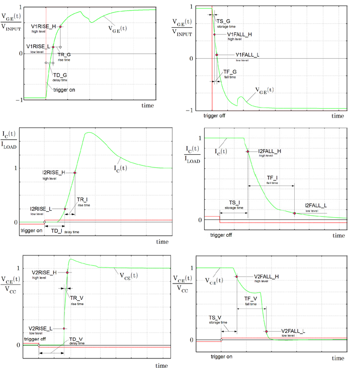
Detailed descriptions of each of these are given below.
QRR
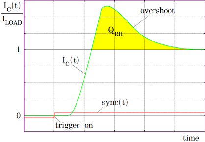
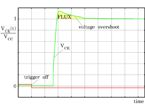
Flux
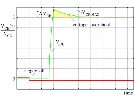
Another integral value is the area under the voltage
overshoot. Define the voltage overshoot as 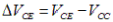 , then
 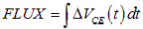 if the voltage overshoot is positive or maximum until
the next on switch trigger occurs. This overshoot is caused by stray
inductances of the circuit from the power source to the half bridge,
throughout the half bridge back to the power source ground. From FLUX
it is possible to calculate the effective stray inductance
if the voltage overshoot is positive or maximum until
the next on switch trigger occurs. This overshoot is caused by stray
inductances of the circuit from the power source to the half bridge,
throughout the half bridge back to the power source ground. From FLUX
it is possible to calculate the effective stray inductance . Using FLUX module
stray inductances can be adapted to the best fit.
. Using FLUX module
stray inductances can be adapted to the best fit.
Cos
To adopt the parasitic capacitances and the charge
controlling life time parameters TAUFD and TAUBE according to given  values of
  this relative collector
current overshoot goal value
this relative collector
current overshoot goal value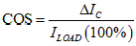 is useful.
COS strongly depends on the reverse recovery current
slope  at the
moment of zero crossing and thus on the total inductance
at the
moment of zero crossing and thus on the total inductance  of the current commutation
path. Both values, COS and the overshoot duration, fit to preserve the excess charge QRR.
of the current commutation
path. Both values, COS and the overshoot duration, fit to preserve the excess charge QRR.
Vos
The voltage overshoot is sensitive to the stray inductances
 and
and  values. It can be
used to fit for the most appropriate circuit stray inductance.
values. It can be
used to fit for the most appropriate circuit stray inductance.
Its definition is 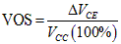 .
.
TxG, TxI, TxV
Here four trigger points and their times used. Starting
from Low come delay, rise, storage and fall time. This simple definition
is applied to the input wave form  , the output current
  and the output voltage
  .
.