
Nominal Working Point Values

The nominal working point of the device is the point commonly used when testing a device for switching parameters such as switching speed, rise time, and delay. Ideally, this point should be the condition in which you are planning to operate the IGBT, but it is more important to have all the data necessary for the characterization available at these conditions. Look to the area of the manufacturer's specification regarding the test conditions for the switching times and losses to locate the Nominal Working Point conditions.
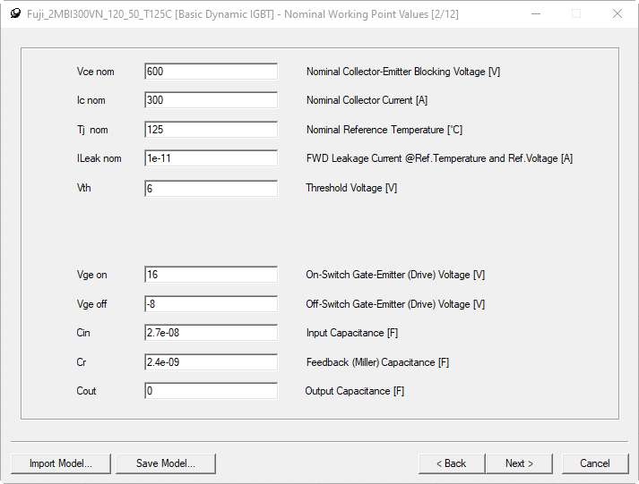
Enter the information required to define the Nominal working point for the device:
Nominal Working Point Values for IGBTs
Nominal Working Point Values for Power MOSFETs
Nominal Working Point Values for IGBTs
Nominal values are the basis of working point dependency.
See Vendor-Specific Guidelines for Nominal Working Point Values below when making the following settings.
|
Nominal Collector Emitter Blocking Voltage [V] |
This is listed as Vcc in the test conditions area of the switching characteristics section of the datasheet. |
|
Nominal Collector Current [A] |
Listed as Ic in the switching characteristics test conditions. |
|
Nominal Reference Temperature [oC] |
This is generally listed as Tc for the maximum temperature test conditions for the switching characteristics, for example 125oC. |
| FWD leakage current under Nominal Conditions [A] | This value should remain at the default value unless specified in the manufacturer’s specification. This parameter directly set the FWD leakage current in the extracted device model. It has little influence to static or dynamic fitting of the model. |
| Threshold Voltage [V] | Listed in table of characteristics. |
|
Collector-Emitter Saturation Voltage under Nominal Condition [V] |
Listed as Vce sat in the switching characteristic test conditions. This field is available only for the Average IGBT characterization. |
|
On-Switch Gate-Emitter (Drive) Voltage [V] |
Listed as Vge in the switching characteristics test conditions. |
|
Off-Switch Gate-Emitter (Drive) Voltage [V] |
This parameter may be listed in the switching characteristics test conditions; however, it often is not. A rule of thumb is to use the negative of the Vge(On) value listed above. |
| Input capacitance [F] | Listed in table of characteristics. |
| Feedback capacitance [F] | Also known as reverse transfer capacitance or Miller capacitance. Listed in table of characteristics. |
| Output Capacitance [F] | Listed in table of characteristics. |
Vendor-Specific Guidelines for Nominal Working Point Values
See these vendor-specific guidelines when setting nominal working point values:
|
Vendor |
Guidelines |
|
ABB |
Most information will be available at 125o C in a datasheet. Review the conditions for which the switching times and energies are given and choose the one in which you want to operate. |
|
Hitachi |
Most information will be available at 125o C in a datasheet. Review the conditions for which the switching times and energies are given and choose the one in which you want to operate. |
|
Infineon |
Most information will be available at 125o C or 150o C in a datasheet. Review the conditions for which the switching times and energies are given and choose the one in which you want to operate. |
|
IXYS |
Most information will be available at 125o C in a datasheet. Review the conditions for which the switching times and energies are given and choose the one in which you want to operate. |
|
Mitsubishi |
Most information will be available at 25o C in a datasheet. Review the conditions for which the switching times and energies are given and choose the one in which you want to operate. Though the information can be limited, it is best to pick the point where the most information is available. |
|
Semikron |
Most information will be available at 125o C in a datasheet. It is good to look at the conditions in which the switching times and energies are given and pick the one in which you want to operate. |