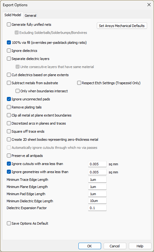
Setting Solid Model Options
To set solid model options:
- Click Export.
- From the 3D Exports area, click 3D Export Options to open the Export Options window.

-
To set the optimal settings for Ansys Mechanical, click Set Ansys Mechanical Defaults, or check boxes and/or enter values in the adjacent fields from the following options:
- Generate fully united nets — unites all solid objects in a net into a single solid object. If conductivities of the different metal layers are similar, this option reduces model complexity and solution time. ALinks sets the material of united nets to copper.
- Excluding Solderballs/Solderbumps/Bondwires — After selecting Generate fully united nets, Excluding Solderballs/Solderbumps/Bondwires activates. Check the box to unite all objects of each net, excluding solderballs, solderbumps and bondwires.
- 100% via fill — ignores the hole size and fills the via entirely.
- Ignore dielectrics — omits dielectric layers from the exported 3D model. Check the Ignore dielectrics box to significantly reduce solution time if capacitance values are not required.
- Separate dielectric layers — creates a separate block for each dielectric layer. Do not check the Separate dielectric layers box if the dielectric constants of the dielectric layers in the stackup are similar.
- Unite consecutive layers that have the same material — After selecting Separate dielectric layers, Unite consecutive layers that have the same material activates. Check the box to unite consecutive layers of the same material.
- Cut dielectrics based on plane extents — if plane extents are defined, the resulting dielectric(s) in the solid model will have that shape. By default, the dielectric layers are exported as rectangular objects that encompass the metal.
- Subtract metals from substrate — explicitly subtracts the metal objects from the dielectric(s), as in the previous versions. If this option is unchecked, metals are not explicitly subtracted from the dielectric. This speeds up the solid model generation process.
- Only when boundaries intersect — adds this condition to Subtract metals from substrate.
- Respect Etch Settings (Trapezoid Only) — check this box to export solid models with the cross-section etching values set in the Trace Cross Section window.Note:
Users can create conformal dielectric coatings (i.e., modeling solder masks) that cover the top and bottom metal layers in the design stackup.
To create and export a conformal coat, first create the environment variable SIWAVE_3D_EXPORT_ENABLE_CONFORMAL_COAT_GENERATION and enter the value 1. The Generate Conformal Layers check box appears under the Respect Etch Settings (Trapezoid Only) check box. Checking the box creates the conformal coat, which can import into Electronics Desktop.
As of version 2024 R2, this feature is still experimental and results may be unexpected.
- Ignore unconnected pads — omits any via pads that do not connect to a plane or trace.
- Remove plating tails — ignores traces that are outside the package and are removed during manufacturing.
- Clip all metal at plane extent boundaries — cuts the selected net that extends past the plane extent boundary. Only the portion within the specified plane extent is exported.
- Discretized arcs in planes and traces — creates chords and break the arcs into smaller fragments.
- Square off trace ends — allows the ends of the traces to not have rounded ends upon export. The round trace ends are chopped off.
- Create 2D sheet bodies
representing zero-thickness metal — generates
solid models containing 2D sheet bodies of zero thickness (instead of
3D bodies of finite thickness) representing geometry on metal layers.
Set the layer thickness to zero for any geometry to be modeled
as a 2D sheet (i.e., navigate to Edit > Layer Stack). Models containing only 2D sheet metal solve much faster
than models containing full 3D metal. Note:
Only available for HFSS and solid model exports.
- Automatically ignore cutouts through which no via passes — ignores the cutouts that do not have any via passing through them.
- Preserve all antipads — includes the antipads associated with unselected nets while exporting a 3D model. Sometimes they need to be preserved regardless of whether the associated nets are selected.
- Ignore cutouts with area less than — check this box and enter a value to ignore voids and/or cutouts smaller than specified.
- Ignore geometries with area less than — check this box and enter a value to omit any geometry from the solid model with an area smaller than specified.
- Minimum Edge Length (Trace Plane, Pad, and Dielectric) — enter values in any/all of these four fields remove small, inappropriate faces from dielectric objects that may cause problems in the meshmaker or the solvers. Any face smaller than the specified value will be omitted from the solid model. Specify the units from the following: um, mm, mil, cm, and/or in.
- Dielectric Expansion Factor— enter a value that will increase the size of the resulting dielectric (e.g., enter 0 and the dielectric is exported exactly as the plane extent. Enter 0.1 and the dielectric shape is enlarged by 10% of the plane extent. A value of 0.2 enlarges the dielectric shape it by 20% of the plane extent.). The existence of a board outline will stop the dielectric from being expanded beyond that boundary.
- If appropriate, check Save Options As Default.
- Click OK to save configuration settings.
If using a *.config file to set 3D export options, set environment variables to 1 to select check boxes and 0 to deselect them (e.g., the 100% Via Fill check box is selected by placing TOTAL_VIA_FILL = 1 in the *.config file).
