
PDN Channel Builder
PDN Channel Builder extracts a power delivery network (PDN) model using either SIwave or PSI. It generates a power channel model of a combined die and package. The model includes the Power and Ground nets in the die and the voltage regulator module (VRM).
As a preliminary step, you should create an IC Die Network.
To invoke the PDN Channel Builder simulation in SIwave:
- Click Simulation.
- Click PDN Channel Builder.
- The Dies list allows you to select which dies are included in a simulation using the Yes and No buttons.Important:
SIwave allows selection of multiple dies.
When two or more are selected, their Pin Grouping must be set to either Use die groups defined in layout or Use PLOC.
- The Die Info area allows you to set pin grouping models, per die.
- The Pin Group Summary area lists existing pin groups.
- Select a Part Name and Ref. Des. from the drop-down menus.
- From the Pin Grouping area, use the radio buttons to select None, Use die groups, or Use PLOC.
- If you selected Use PLOC, click PLOC Connection to adjust additional settings. Otherwise, proceed to Step 13.
- From the IC Die Information panel, use the Browse button to locate and select the CPM, PLOC, or Voltus file you want to import.
- Click Auto Connect .
- If appropriate, you can Create Pin Groups in the Package and Die Pins
- If appropriate, you can Export Connection Information to a text file.
- The Operations area contains buttons to Merge selected groups or Merge groups on same net. You can change the reference group for a specified pin to a pin group selected from the drop-down menu. Click Update to update the reference group.
- Click OK to close theApache CPM/PLOC Import window and return to the PDN Channel Builder window, PLOC Connection tab.
- The Pin Group Summary area lists any pin groups in the PLOC component when it is connected.
- The Port Summary area lists any ports in the PLOC component when it is connected.
- The VRM area specifies the components and pins that supply voltage and ground to the die.
- From the VRM area, select the Part and Reference Designator.
- If appropriate, click Save Settings to preserve the parameters for the PLOC connections.
- Select the Channel Components tab.
The Channel Components tab displays.
Review the Channel components. These are passive components mounted on the package (other than the Die and BGA). If any passive component has a capacitor models specified, those component pins are automatically extracted and exposed in the Spice netlist. This helps in studying subsequent what-if scenarios without having to go through the extraction again. If a component contains simple R and L elements, these components are absorbed into the extraction and not exposed at the Spice netlist level.
- Select the VRM Setup tab.
The VRM Setup tab displays.
Specify BGA components and pins that supply voltage and ground to the die. To select parts, use the Part and Ref. Des drop-down menus, or click the gray area adjacent to a row. You can select multiple rows using Ctrl+click.
- Select a Power Net and Ground Net to be extracted, and specify the Supply Voltage. Use the Add Rows and Delete Rows buttons to add and remove parts as appropriate. You can also Restore Recommended VRM Assignments.
- The net with the largest number of BGA component pins is designated as the Reference (Ground) net. Other nets are routed to BGA component, and are terminated with a DC supply voltage of 1.5V by default. This value can be edited independently for each net, and the voltage level can be modified even after the extraction. If a suitable PCB model is available, it can replace the VRM model after the extraction is done.
- The pin groups defined on the BGA component are extracted and VRM supply voltages are distributed to these groups. If no pin groups are defined, all the pins for each net are grouped automatically, and the supply voltages are connected on net-by-net basis.
- Select the Unconnected Die Pins tab.
The Unconnected Die Pins tab displays.
If you previously selected PLOC connections, this tab allows you to specify Supply Voltage values for any unconnected PLOC nets. To update a voltage value, select a net, enter a value in the Supply Voltage field, and click Update.
If you did not select any PLOC connections, the options on this tab will be disabled.
- Select the Simulation tab.
- Use the Solver drop-down menu to select either SIwave or PSI.
- From the Simulation Name field, enter a name or accept the default.
- From the Frequency Range Setup area, add and delete rows as appropriate using the Add Above, Add Below, and Delete Selection buttons.
- Click the cells and enter new values to change the Start Freq., Stop Freq., Num. Points/Step Size, and Distribution.
- From the Sweep Selection area, use the radio buttons to select either Discrete Sweep or Interpolating Sweep.
- If appropriate, check the FWS generation parameters check box
- Click the cell and enter a value to set the Min. Rise/Fall Time.
- From the 3D Solver area, you can use the check boxes to select Q3D or HFSS. Q3D automatically detects regions for inclusion, while HFSS requires you to click and set HFSS solver options.
- If appropriate, click Other solver options to change general solver settings.
- If appropriate, click Save Settings to preserve simulation settings.
- Click OK to start the simulation.
The PDN Channel Builder window opens with the Die Configuration tab selected.
Click through the slides below to see the different tabs.


|
On the Die Configuration tab:
The CPM/PLOC/Voltus Import window appears.
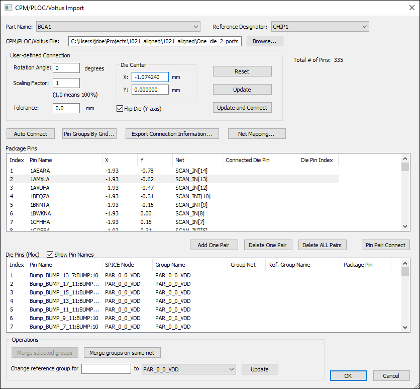
The Package Pins area lists the package pins.
The list of Die Pins populates. Values for Rotationand Location of die center on package are read from the file and displayed. The Flip Die check box setting is determined automatically from data in the CPM file.
The lists of Package Pins and Die Pins are updated to show the connections. The upper-right area of the window displays the number of Pins mapped and the number of Pins unmapped. For a successful auto-connect, all of the pins will be mapped and no pins will be unmapped.
From the Die panel, the Pin Group Summary and Port Summary fields are populated with information from the PLOC file.
For each Part/Ref Des row in the VRM panel, select a Power Net and Ground Net to be extracted, and specify the Supply Voltage. Use the Add Rows and Delete Rows buttons to specify multiple parts or multiple sources.
The Simulation tab displays.
If you choose an Interpolating Sweep, you must enter the Relative Error percentage. Additionally, the Compute exact DC point option becomes available.