Grouping Pins
You can create pin groups for various components. During analysis, grouped pins are treated as if they are electrically connected. You can also connect circuit elements (ports, sources, RLCs) to any generated pin groups. Consult the Technical Notes for a brief walkthrough.
Pin groups can be created multiple ways:
- From the Tools tab
- From the Modeling workspace
- From the CPA setup window (Hotspot Die Pin Group Generation)
Grouping Pins from the Tools Tab
To create a pin group:
- From Tools, select Create/Manage Pin Groups
to open the Create/Manage Pin Groups>window.
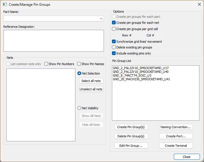
- From the Part Name drop-down menu, select a part. To display all pin groups in the design, select DON'T KNOW.
- The Reference Designator area will populate. Make your appropriate selection(s).
- From the Nets area, use the radio buttons to select either Net Selection or Net Visibility.
- To select all the nets, click Net Selection and then click Select all nets. The pins associated with the selected nets will be grayed.
- To show all the nets in the Modeling workspace, click Net Visibility and then click Show All Nets.
- Also in the Nets area, use the check boxes to narrow your search by listing common nets only, or decide whether to show pin numbers and names.
- Select the Nets you want to include in the pin group.
- From the Options area, select the settings for your pin group:
- Create pin groups for each part – Use this option if the selected part contains multiple reference designators and you want to create identical pin groups for each of them.
- Create pin groups for each net – Use this option if multiple nets are selected and you want to generate multiple pin groups (one for each selected net).
- Create pin groups per grid cell – Use this option if you know the grid location where you'd like to create the pin group. Enter the row and column number to update the Modeling workspace.
- Synchronize grid lines' movement – Use this option to synchronize the movement of grid lines.
- Delete existing pin groups – Use this option to delete existing pin groups when creating a new group. Existing groups display in the Pin Group List.
- Include existing pins only – Use this option to only include existing pins in the selection when creating or editing pin groups.
- Optionally, click Naming Convention to change the naming convention for circuit elements.
- Optionally, use the Create Port and Create Terminal buttons to create ports and terminals for inclusion in your group.
- Click Create Pin Group(s).
The created groups display in the Pin Group List.
To delete a pin group:
- From the Pin Groups area, select the group you want to delete.
- Click Delete Pin Group(s).
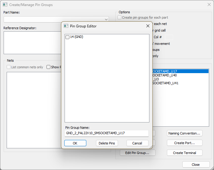
To edit a pin group:
- From the Pin Groups area, select the group you want to edit.
- Click Edit Pin Group to open the Pin Group Editor window. From the Pin Group Editor window, rename the group or delete pins.
Grouping Pins Quickly in the Modeling Workspace
As an alternative to the preceding instructions you can group pins without opening the Create/Manage Pin Groups window.
To do this:
- Ctrl+click to select pins in the Modeling workspace.
You can also select pads and vias.
If a subset of the selection is already part of an existing single component, SIwave will add selected pads/vias that do not have pin assignments to this existing component.
If a subset of the selection belongs to more than one component, pads/vias without pin assignments will be added to the parent component of the first selected pin and a pin group spanning these different components will be created.
If none of the pads and vias have pin assignments, a new component is created to act as the parent for the new pins.
Important:A pin group containing pins from multiple components will not work in CPA.
- Right-click to open the options menu.
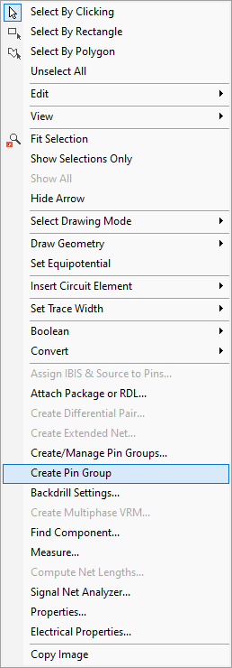
- Click Create Pin Group.
The pins are grouped, and the pin group properties display in the Properties workspace.
- Pin groups on the die side are treated as sources while pin groups on the ball side are sinks. If you only have pin groups defined on the ball side, the resulting matrix will contain individual terminals for the die side sources.
- Pin groups should be defined on signal nets. Pin groups created on nets that are defined as power/ground are not included in the resulting matrix.
Grouping Pins from CPA (Smart Pin Groups)
For CPA RLGC extraction, you can generate pin groups based on hotspots. This is more efficient than extracting every pin.
To generate pin groups automatically:
- Click Simulation.
- From the CPA area, click Compute RLGC to open the Launch CPA window.
- Select CPA Channel Setup.
- From the Extraction Type area, select Hotspot Die Pin Group Generation.
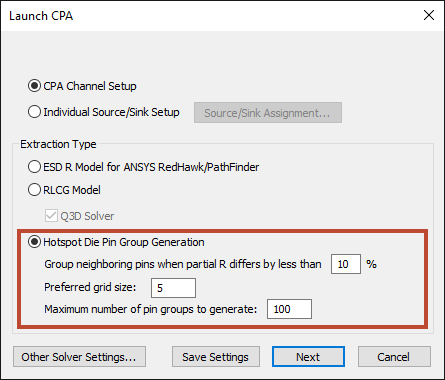
- Enter a percentage value to group neighboring pins when their partial resistance differs by less than that percentage from the nominal value. The default is 10%. Pins that fall outside this range are put into single pin groups (extracted individually).
- Enter a Preferred grid size. The default is 5. Pins with partial resistance within the specified range are further put into a grid of 5x5 (default), and are grouped by net.
- Enter a value for the maximum number of pin groups to generate.
- Click Next
to open the SIwave-CPA Simulation window, with Hotspot-specific options.
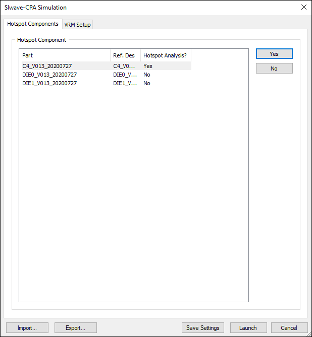
- Select parts and use the Yes and No buttons to assign whether or not they will be part of the Hotspot grouping. Parts are set to "No" by default.
- Select the VRM Options tab and choose options as appropriate.
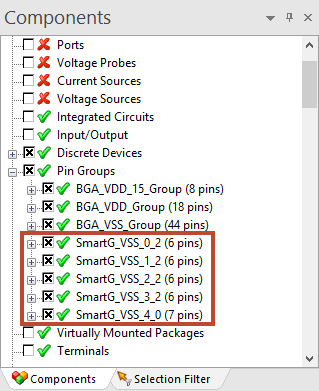
- Click OK and the Messages window updates with a progress bar. When the progress bar is finished, the pin groups are created and listed in the Components window. Pin groups created using smart grouping begin with the prefix 'SmartG'.
 Note:
Note:If there are existing pin groups on a die component, SIwave will prompt you to determine whether to overwrite the existing groups.
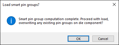
Click OK to overwrite the pin groups. Click Cancel to abort.
