
Running Simulations in DDR Wizard
To run a cosimulation in DDR Wizard:
- Click Simulation > DDRwizard.
DDR Wizard opens in a new window, on its Basic Setup screen:

- Use the drop-down menus to select the DDR Type, Speed, and Command Rate. If appropriate, you can manually enter a custom speed.
- If appropriate, click Auto Identify to reclassify nets into new groups after updating the group identifiers (search string for group) in DDR Wizard Settings.
- If appropriate, manually select or deselect nets in the table. Only selected nets will be analyzed.
By default, all nets classified as DQ, DQS, ADDR, and CLK are selected; nets classified as OTHER are deselected.
Note:Differential nets populate the Differential column, Extended nets populate the Extended column, and Differential-Extended nets populate both.
- To update Strobe/Clock and Delay, highlight one or more rows and use the drop-down menus in the Operations area.
- If appropriate, select the Ideal Components check box. This forces all ICs to have no IBIS model, and removes VRMs. Selecting Ideal Components also disables the Ideal Power check box in the next phase of setup (see: Step 9).
- If appropriate, use the Voltage drop-down menu to customize the Vdd value and apply to all sources.
Note:
When IBIS model is present on the driver, DDR Wizard applies voltage of 1V.
- If appropriate, click Save Configuration File to save your settings as a *.ddx file. These files can be loaded using Load Configuration File.
- Click Next.
DDR Wizard updates to display the IBIS Setup screen:

This screen lists all components from nets selected on the previous screen.
Driver and Receiver are automatically assigned with the IC with more pins being the driver. IBIS components are also automatically assigned based on IC properties. However, all of these settings can be changed using the options in the Operations area.
If a new IBIS component is assigned, the IBIS models are automatically assigned to individual pins in the IC based on pin name match between the IC pins and IBIS component pins. Unmatched pins are assigned to the first single-ended model or the first differential model in the IBIS component.
- If appropriate, change a component's Type and Corner, or specify an IBIS Component.
Note:
When IBIS components are specified, you can change the IBIS model on the Read Mode and Write Mode tabs.
- If appropriate, enable Perform sweep across all corners. From the Electronics Desktop simulation setup, a sweep is set up to use typical, minimum, maximum, fast, and slow. Reports generate five curves instead of one for every probe.
- If appropriate, enable Ideal Power to remove VRMs.
- Use the radio buttons to select whether IBIS models are assigned based on IBIS Pin Name Match or Net Group.
- If appropriate, click the DQ/DQS Read Mode, DQ/DQS Write Mode, or ADDR/CLK/OTHER tabs to view more information.


Drivers and receivers are chosen automatically, but can be changed.
- In DQ/DQS Write mode, the component with the largest number of pins is chosen as the driver. Thus the main microcontroller or the DIMM connector is usually the driver and the Memory ICs are the receiver.
- In DQ/DQS Read mode, the opposite is true.
- On the ADDR/CLK/OTHER tab, the driver and receiver sides are initially chosen the same as in DQ/DQS Write mode, but can be independently changed.
The IBIS models assigned for DQ/DQS drivers will be the DRV models and for DQ/DQS receivers will be the ODT models.
When IBIS components are specified on the IBIS Setup tab, the IBIS Model can be changed from the DQ/DQS Read Mode, DQ/DQS Write Mode, or ADDR/CLK/OTHER tab.
The IBIS component and IBIS model can be regular IBIS (defined using a .ibs file) or IBIS AMI (defined using .ibs/.ami/.dll/.so files)
- Click Next.
If Ideal Power was selected on the previous window, proceed to Step 16.
If Ideal Power was not selected on the previous window, ]DDR Wizard updates to display Component and Ground Nets.

Select one or more part(s) and use the Operations area to set:
- Power Supply
- Power Net
- Ground Net
- Power Net Pin Grouping
- Ground Net Pin Grouping
If there are no VRM parts, proceed to Step 16.
If the chosen Supply for any part is VRM, the DDR wizard displays a VRM Parameters step.
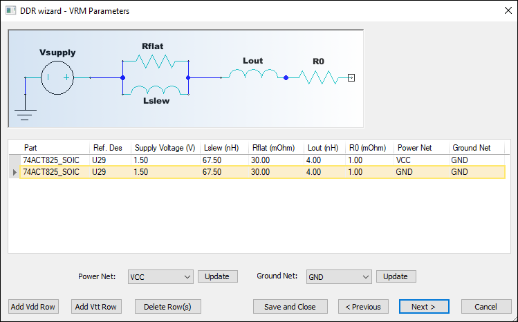
Here, you can adjust the Power Net and Ground Net for each VRM part.
- Click Next.
The DDR Wizard updates to display Transient Simulation Options:

This step includes options for:
- Project Name – the name of the schematic generated in Electronics Desktop.
- Use Ansys Electronics Desktop-SIwave Dynamic Link – enable dynamic link.
- Use SSS Model – enable state space model.
- Use Touchstone Model – enable touchstone model.
- Step Size – specify the value and unit.
- Stop Time – specify the value and unit.
- Invoke Transient Simulation – select whether to invoke Transient simulation. This option must be enabled in order to use AMI sources.
- Plot Driver Waveforms – select whether driver waveforms are plotted.
- Plot Receiver Waveforms – select whether receiver waveforms are plotted.
- Plot Power Rail Waveforms – select whether power rail waveforms are plotted.
- Invoke QuickEye Simulation – select whether to invoke QuickEye simulation.
- Plot Eye Waveforms – select whether to plot Eye waveforms.
- S-Parameter Options – enter reference impedance values and specify a frequency sweep by clicking Edit. See: Computing Frequency Sweep.
For more information on AMI, QuickEye, and Transient, consult the following sections of the Circuit Help:
Note:Electronics Desktop supports the use of DDR variables.
- Assign settings as appropriate.
- Click OK.
SIwave generates two schematics (one for Read mode and one for Write mode), which open in Electronics Desktop.
Each schematic contains multiple tabs:
- Main tab – the center displays the dynamic link block. Voltage sources and VRMs appear at the top. IBIS component sub-circuit blocks display to the sides.
- Subsequent tab(s) – contain driver/receiver blocks with each byte lane along with corresponding strobe. These are in individual tabs, organized by DQ/DQS, ADDR/CLK/OTHER, and IBIS. The number of tabs varies by schematic.
Click through the slides below to see the tabs. Click an area highlighted in green to enlarge it in a new window.


