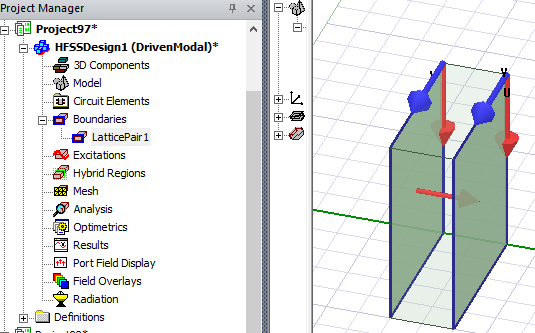
Assigning Coupled Lattice Pair Boundaries
Coupled Lattice Pair boundaries enable you to model planes of periodicity where the E-field at every point on the Secondary boundary surface is forced to match the E-field of every corresponding point on the Primary boundary surface to within a phase difference. The transformation used to map the E-field from the Primary to the Secondary is determined by an auto-set coordinate system for the coupled lattice pair. The boundaries are useful in creating unit cells and arrays. (You can also assign Primary and Secondary boundaries for a coupled lattice pair separately.)
To assign a Coupled Lattice Pair:
- Select two surfaces
on which to assign the coupled lattice pair and click HFSS>Boundaries>Assign>Couple...>Lattice Pair...to bring up the Lattice Pair
dialog box.
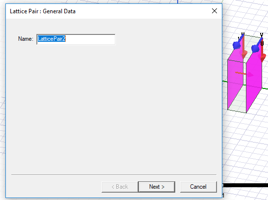
- Click Next.
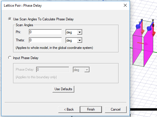
You have the option to relate the Secondary boundary's E-fields to the Primary boundary's E-fields in one of the following ways:
For driven designs, select Use Scan Angles to Calculate Phase Delay to enable the Scan Angle fields. Then enter Phi and Theta scan angles. These apply to whole model, in the global coordinate system. The phase delay is calculated from the scan angles; however, if you know the phase delay, you may enter it directly in the Phase Delay box.
Note: Note: For Eigenmode problems, the Use Scan Angles to Calculate Phase Delay fields are disabled.Select Input Phase Delay, and then enter the phase difference, or phase delay, between the boundaries' E-fields in the Phase Delay box. The phase delay applies only to this boundary.
Note: : You can assign a variable as the phi, theta, or phase delay values.
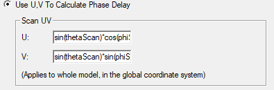
A Beta Option allows you to Use U,V to Calculate Phase Delay.
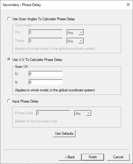
This permits you to scan to scan in the invisible range which is conveniently specified by u,v coordinates. U or V can span anything between -infinity to + infinity or practically some large negative value to large positive value. When U2+V2 > 1, it is the invisible range. You can specify U and V as equations in this form:
u = sinθ∙cosφ
v = sinθ∙sinφ
Note that you can employ variables in the equations:
Ansys Electronics Desktop will compute the E-field on this boundary and map it to the Secondary boundary using the transformation defined by the Primary and Secondary coordinate systems.