


In-Circuit Testing (ICT) uses a collection of test probes and test fixtures on one or both sides of a circuit card to test electrical connections during the manufacturing process. Each test probe exerts a mechanical force on a specific circuit card location, called the test point, as determined by the design. The combined effect of all these test point forces displaces the circuit card during the test, causing mechanical stresses to be experienced by each solder joint. If the stress values are high enough one or more solder joints could fail. The ICT Analysis module provided by Ansys Sherlock models the mechanical stresses exerted by the test points and fixtures and scores each circuit card part based on the predicted stresses for that part.
In this section, the following topics are covered:
The ICT Analysis Module makes use of the following input data for the analysis calculations:
Parts List
Tip: The following section explains which part properties Sherlock uses in the ICT analysis: Tables: Required Part Properties per Analysis Type.
Size and location of all parts, plated through-holes, and cutouts
Size and location of all test points and test fixtures
Circuit card mechanical properties (stackup data)
Circuit card outline
Mesh Properties.
If any of the input data listed above is changed, Sherlock will automatically clear the analysis results for this analysis module.
Warning: Exercise caution when using multiple versions of Sherlock on the same project. To avoid inaccurate results, see the section Compatibility with Earlier Versions of Sherlock.
ICT analysis depends on the current placement and type of ICT Fixtures associated with the circuit card being analyzed. See the section on Mount Points & Fixtures for details concerning the creation and management of ICT Fixtures.
Much like ICT Test Fixtures, the test points used by the ICT Analysis Module can be added, modified and deleted using the Test Point Editor provided by the CCA Layer Viewer. To access the Test Point Editor:
Double-click the Inputs > Layers entry for the circuit card being analyzed to display the Layer Viewer
Select Edit > Edit Test Points from the main menu of the CCA Layer Viewer
At that point, the Test Point Editor buttons will be displayed at the bottom of the Layer Viewer, as shown in the following screen shot:
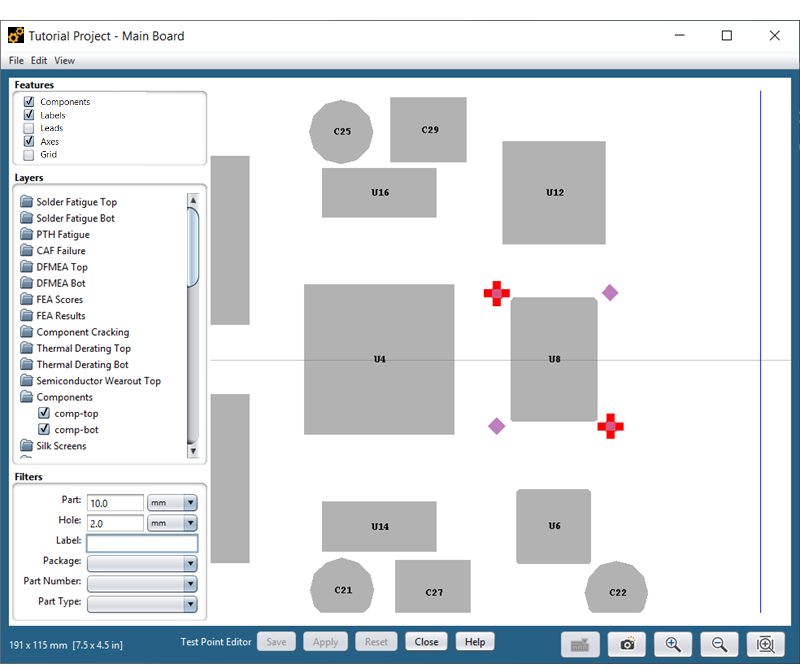
In this case, four test points are shown as purple diamonds located near the corners of part U8. Two of the test points have been selected for editing, as denoted by the red outlines and corner nodes. Single or multiple test points can be selected using the same keyboard and mouse iterations described for test fixtures.
Note: By default, test points are displayed as purple diamonds in the Layer Viewer. You can customize the color using the Settings > Color Settings option in the Main Menu.
To add a test point, simply right-click on the circuit card at the approximate location for the test point and select Add Test Point from the context menu. At that point, the Add Test Point dialog will appear, indicating the default properties to be assigned to the new test point, as shown below.
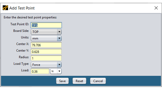
You may specify the exact location using the Center X and Center Y fields or you may simply move the fixture to the proper location after it has been created. Other than the Board Side and Force values, all other test point properties can be edited using either the dialog form or graphical controls (discussed in the next sub-section).
Note: The Test Point ID must be a unique value for each test point. Sherlock automatically selects an available ID, but you are free to use whatever ID you want.
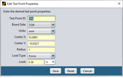
To move one or more selected test points, left-click inside of any selected test point and drag the test point(s) to the new location. To resize one or more test points, left-click any of the highlighted corners and drag that corner to change the size of all selected test points. Finally, to access the context menu for one or more selected fixtures, right-click inside of any selected fixture to display the following menu items:
Edit Properties
Move Test Point(s)
Scale Test Point(s)
Delete Test Point(s)
Other than Edit Properties, the menu items are self-explanatory. When the Edit Properties menu item is selected for a single test point, the Edit Test Point Properties dialog will be displayed (see below) and will be identical to the Add Test Point dialog shown above. Simply modify the desired test point properties and press Save to update the test point.
When multiple test points are selected, only a subset of the test point properties will be editable, as shown here. For each property shown, if the value is the same for each selected test point, then that value will be displayed. Otherwise, <VARIOUS> will be shown in the property field to indicate that the selected test points have different values for that property.
To modify one or more property values for all selected test points, simply update the property field(s) and press the Save button. At that point, all selected test points will be updated. If <VARIOUS> is specified for a given property value, then no changes will be made to that property in any of the selected test points.
After adding, modifying or deleting test points, you should press the Save or Apply buttons at the bottom of the Layer Viewer to save your changes. The Apply button will save the changes but keep the Test Point Editor open, allowing you to make additional changes. The Save button saves the changes and automatically closes the Test Point Editor.
ICT Test Points can be imported from the following types of design files:
Test Point (CSV) - comma separated file containing test point data
Pick & Place (CSV) - comma separated file containing pick & place data
Pick & Place (DELIMITED) - delimited file containing pick & place data
Pick & Place (FIXED) - Fixed column file containing pick & place data
Pick & Place (ODB++) - ODB++ file containing pick & place data
In the first (most common) case, a spreadsheet file is used to provide the test point data, while in all other cases the test point data is extracted from the Pick & Place data by looking for reference designators starting with a specific Test Point Prefix.
For example, consider the following CSV file:
| "Test Point Example" |
| "X","Y","Board Side","Force" |
| 1,1,"TOP",5.2 |
| -1,-1,"BOTTOM",0.36 |
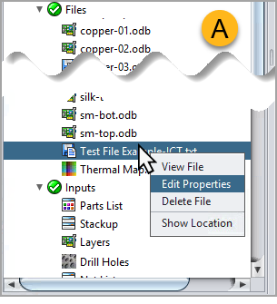
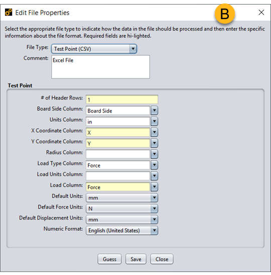
To add a file to the CCA, either select from the main Sherlock menu, or right-click Files and select Add File(s) from the Project Tree as shown below (A). To assign a file type, open the Edit File Properties dialog (B, below) by right-clicking the file, selecting Edit Properties, and then toggling the File Type drop-down menu.
The two test points are defined, providing their X, Y coordinates (required), board side (optional) and force (required). The test point data from this file can be imported into Sherlock by selecting the Test Point (CSV) file type in the Edit File Properties dialog shown below. At that point, the list of properties will be displayed, allowing you to specify the columns to be used for specific data. In many cases, Sherlock will automatically guess the appropriate columns, but you may have to specify one or more columns depending on the column headers defined in the file.
When the Save button is pressed, Sherlock will parse the file and add all the test points found. For identification purposes, Sherlock assigns a string ID starting with TP to all test points defined in the file.
In some cases, the Pick & Place design files associated with a given circuit card will contain entries for some or all of the test points defined for that circuit card. In such cases, Sherlock can be used to automatically import test point definitions from the Pick & Place data and create corresponding test points with default properties. For example, consider the following Pick & Place spreadsheet file:
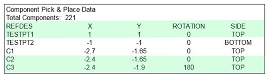
In this case, two test points are defined using the TESTPT prefix in their reference designators, providing their X,Y coordinates and the side of the board on which they are located.
After examining the file contents, you need only specify the prefix used by the test point definitions as one of the file properties in the Pick & Place (CSV) edit dialog, as shown below.
When Sherlock imports the Pick & Place data it will automatically treat all reference designators starting with that prefix as a test point and will create a default test point accordingly. Then, you need only select groups of test points and set their forces to complete the input process.
The ICT Analysis Module creates a finite element model by creating a mesh that includes all selected parts, holes, cutouts, test fixtures and test points. You can display the current ICT mesh by selecting the ICT Mesh layer (if available) in the Other Layers folder of the CCA Layer Viewer. You may also re-create the ICT mesh at any time by selecting Edit > Update ICT Mesh from the Edit menu in the CCA Layer Viewer.
Note: When examining the ICT mesh, you might notice that fixtures are meshed just as parts are, but no such mesh exists for test points. Instead, test points are modeled by a single mesh node located at the test point coordinates. This may disrupt the appearance of the surrounding mesh but is required to accommodate the single node location. A single node is used because the ICT Analysis module assumes the force is applied at a single point.
The following optional settings enable you to customize the ICT results. To enable or disable a feature, navigate to the Analysis Settings panel by clicking from the main menu. See Analysis Properties Settings for more information.
Report Microstrain: When ENABLED (default setting), Sherlock reports ICT analysis results in terms of microstrain. You may toggle this setting on or off.
Collect Additional Strain Data: By default, this option is turned off. When ENABLED, the Sherlock application collects and reports max directional and principal surface strains in addition to other strain data when performing the ICT analysis. You can view this data in the Layer Viewer and the Results Tables. For this feature, the source of the data is elemental nodal values by element, but the data in the Results Table and Layer Viewer is the averaged elemental nodal values for nodes on the given surface.
This Collect Additional Strain Data feature is only available when the Ansys FEA engine is selected. See FEA Engine.
For more information on analysis results, see ICT Analysis Results below.
The ICT Analysis task can be executed whenever the following requirements are met:
At least one test fixture is defined
At least one test point is defined
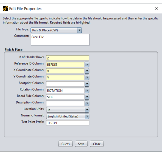
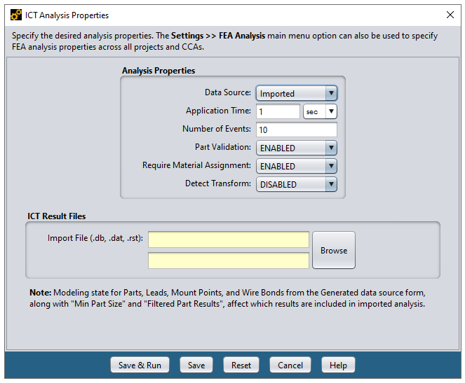
To edit the analysis properties, right-click the ICT Analysis entry in the Project Tree and select the Edit Properties menu item to display the ICT Analysis Properties dialog. As a convenience, you can also run the analysis immediately, using the last properties entered, by selecting the Run Analysis Task option from the context menu.
When using the Generated data source (A, below), you may specify mesh properties using the various settings in the PCB Modeling form (B). See the FEA Overview for more details.
Unlike other FEA analysis tasks, ICT analysis does not use any Life Cycle Events. To provide Time-to-Failure Calculations, the Application Time property combined with the maximum component strain are used.
Application Time (C) is the time it takes to apply the load– that is, the time between no load to full load.
Number of Events (D) specifies the number of times the load is applied.
ICT analysis results can be imported into Sherlock by selecting Imported for the data source (A, below). When selected, you simply enter the locations and names of the FEA model and results files.
The supported file types are *.db, *.dat, and *.rst.
Tip: For detailed, step-by-step instructions for importing results from Ansys Workbench, see the following section: FEA- Ansys Workbench™ Integration.
The Detect Transform property (B) is located under the ICT Analysis Properties. When the Detect Transform is ENABLED, Sherlock will attempt to detect any Transforms applied to the imported model and make adjustments if required. This ensures the imported model matches Sherlock's original model. Select MANUAL to enter Transform properties manually. If a Transform exists and is not detected, Sherlock will not be able to provide component results. When running the Detect Transform feature, Sherlock uses multiple threads by default. To learn more about this feature and how to adjust it, see Transform Detection Threading under FEA Analysis Settings.
When the Save & Run button is pressed, Sherlock will import both the model and the results to determine the reliability results.
Note: If lead results are not generated after importing results which contain leads, do the following: Enable Lead Modeling on the Generated Data Source form (shown above) and perform the imported analysis again.
The results generated by the ICT Analysis Module show the maximum displacement and strain experienced by each component during the analysis, as well as the location and force or displacement of each test point. The analysis results are used to assign a score to each part and a combined score for the circuit card itself. Sherlock displays a summary panel showing the overall scores and range of bending forces experienced by the board, as well as a table showing individual results for all parts associated with the circuit card. We now describe each analysis result in more detail.
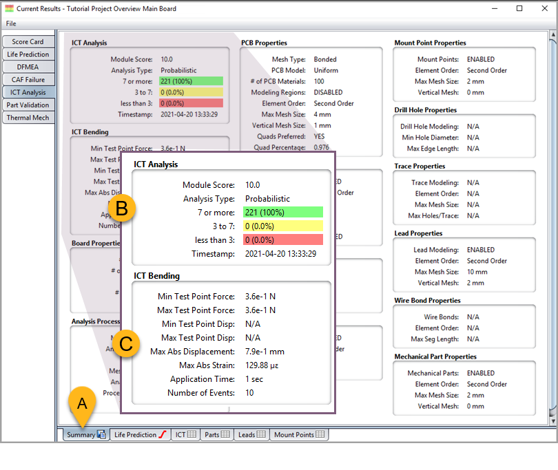
When the ICT Analysis process is finished, a GREEN check mark will appear next to the ICT Analysis entry in the Project Tree. Double-click that entry to display the ICT Analysis Results panel and select the Summary sub-tab (A, below).
The Summary Panel (B) shows the overall distribution of scores assigned to each part analyzed, along with the overall score assigned to the circuit card itself.
The ICT Bending (C) panel shows the minimum and maximum test point forces and test point displacement applied to the board, and the maximum displacement and strain predicted by the ICT analysis model. It also includes the Application Time and Strain per Event used as analysis inputs.
The PCB Properties, Analysis Process, and various Mesh Properties panels show the statistics for the number of inputs and properties used for the analysis.
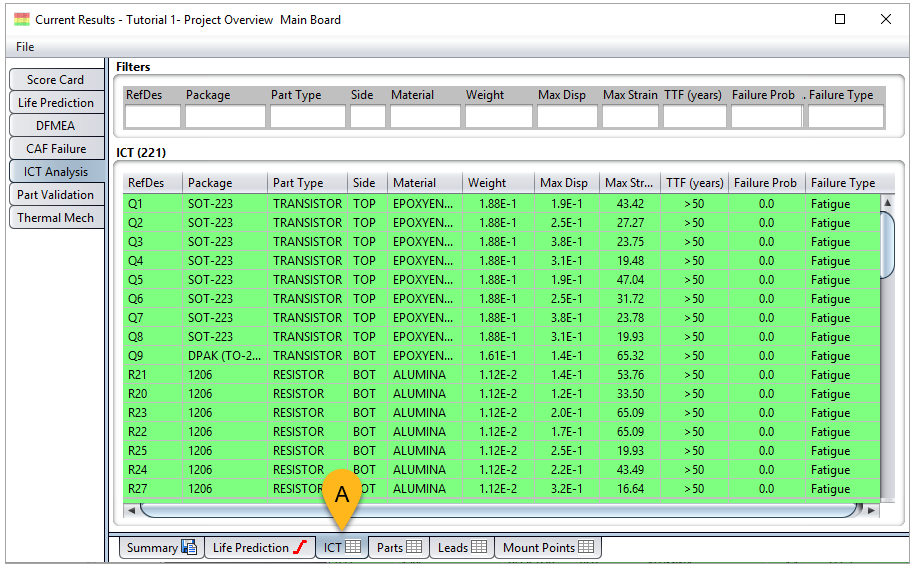
Select the ICT Table sub-tab (A, below) to examine the detailed results generated for each part analyzed.
The table rows are color-coded based on the score assigned to each part, which is based primarily on the maximum strain experienced by that part according to the ICT model. As with all other Sherlock tabular results, you can double-click any row to view the properties associated with a given part and/or select one or more rows to be exported to a CSV file. See the section on Data Export for more details.
If you enabled the Collect Additional Strain Data feature (see above, ICT Results Settings), the source of the data is elemental nodal values by element, but the data in the Results Table is the averaged elemental nodal values for nodes on the given surface.
Tip: Remember, you can customize the Results Table so it displays results in microstrain, and you can have the table display max directional and principal surface strains in addition to other strain data. You must apply these settings before running the analysis. See above, ICT Results Settings.
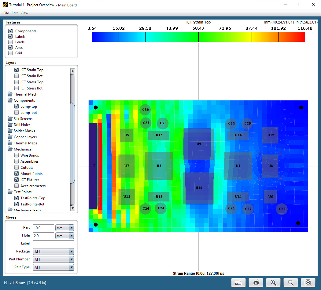
The analytic results and scores generated by the ICT Analysis Module can be viewed graphically using the CCA Layer Viewer shown below. The layer shows the combined strain (in both the X and Y directions) predicted over the board surface for the given test point forces:
In addition to the strain results, we've selected the ICT Fixture, Test Point and Component layers so that we can fully understand the results. With a single test fixture located along the left side of the board and four test points located near the right side of the board, the maximum strain values are seen near the text fixture, as expected. The red areas also show relatively high strain values in between the large components.
The raw results shown by the displacement and strain layers is useful for validating the analysis model, but they don't clearly show how each component is affected by the predicted strains. To see clearly how each part is affected, we can examine the score layers generated by the ICT Analysis Module. In this case, the score assigned to each top component is shown in a color-coded region.
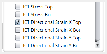
Tip: The Layer Viewer can also display max directional and principal surface strains as explained earlier. To do so, you must enable the Collect Additional Strain Data feature before running the analysis. See above, ICT Results Settings. When enabled, you can visualize directional strain data in the Viewer by selecting one of the relevant options as shown below. The source of the data is elemental nodal values by element, but the data shown in the Layer Viewer is the averaged elemental nodal values for nodes on the given surface.
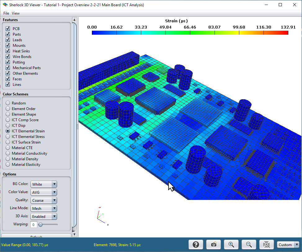
You can view the 3D FEA model and/or results by right-clicking the ICT Analysis node in the Project Tree and selecting either the View 3D Model or View 3D Results option from the context menu. In both cases, the Sherlock 3D Viewer will be launched, as shown below, allowing you to interactively view the 3D data. See Viewing and Managing Analysis Results for more details.
Note: In the 3D Viewer, when viewing any of the color schemes related to material properties (Material CTE, Material Conductivity, Material Density, and Material Elasticity), the values represented are for the material at 20°C only.
If the Show FEA Logs option is enabled in the Settings > FEA ANALYSIS dialog, then a Log Panel will be displayed along with the other analysis results containing the log generated by the FEA engine during the analysis process. Advanced users can review such log data to determine if everything was processed as expected and/or to trouble-shoot FEA processing issues.