


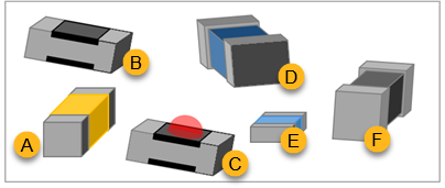
Chip Components (CC) are leadless packages which include resistors, ceramic capacitors, ferrite beads, and diodes.
Note: There are special considerations for resistor networks or capacitor arrays. See the section below Resistor Networks and Capacitor Arrays.
| ID Tab |
|
Chip Component Properties:
| Package Tab | |||||||||||||||||||||||||||||||||||||||||||||||||||||||||||||||||||||||||||||||||||||||||||||||||||
| |||||||||||||||||||||||||||||||||||||||||||||||||||||||||||||||||||||||||||||||||||||||||||||||||||
| Lead Tab |
|
| Pad Tab |
|
PCB artwork, when available, supercedes pad dimensions given by a data sheet or a standard. Tip: If you have a completed Sherlock model, use the Update Pad Properties Tool in Sherlock which is designed to automate entering pad properties. |
|
This table shows recommended pad dimensions for CC Resistor, Inductor, and Capacitor parts. It is included for reference. PCB artwork should be used as the input! | |||||
| CC Component | Length | Width | Pad Length | Pad Width | Pitch |
| 01005 | 0.4 | 0.2 | 0.18 | 0.2 | 0.3 |
| 0201 | 0.6 | 0.3 | 0.3 | 0.3 | 0.6 |
| 0306 | 0.8 | 1.6 | 0.5 | 1.6 | 0.8 |
| 0402 | 1 | 0.5 | 0.5 | 0.5 | 1 |
| 0508 | 1.2 | 2 | 0.8 | 2 | 1.2 |
| 0603 | 1.6 | 0.8 | 0.8 | 0.9 | 1.6 |
| 0612 | 1.6 | 3.2 | 1 | 3.2 | 1.6 |
| 0805 | 2 | 1.2 | 1.3 | 1.3 | 2 |
| 1008 | 2.7 | 2 | 2 | 1 | 2.7 |
| 1020 | 2.5 | 5 | 1.3 | 5.5 | 2.5 |
| 1206 | 3.2 | 1.6 | 1.6 | 1.6 | 3.2 |
| 1210 | 3.2 | 2.5 | 1.6 | 2.5 | 3.2 |
| 1218 | 3.2 | 4.5 | 1 | 4.6 | 3.2 |
| 1225 | 3.2 | 6.4 | 1.7 | 6.4 | 3.2 |
| 1806 | 4.5 | 1.6 | 1.7 | 1.6 | 4.5 |
| 1812 | 4.5 | 3.2 | 2 | 3.2 | 4.5 |
| 1825 | 4.5 | 6.4 | 2 | 6.4 | 4.5 |
| 2010 | 5 | 2.5 | 2 | 2.6 | 5 |
| 2030 | 5.1 | 7.6 | 2 | 7.8 | 5.1 |
| 2220 | 5.7 | 5 | 2 | 4.2 | 5.7 |
| 2225 | 5.7 | 6.35 | 2 | 6.35 | 5.7 |
| 2512 | 6.4 | 3.2 | 2 | 3.2 | 6.4 |
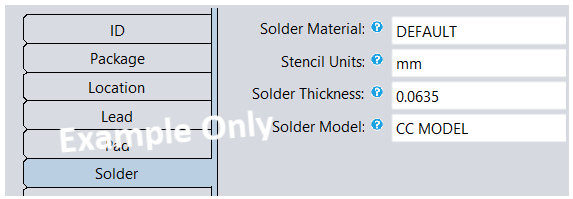
| Solder Tab |
|
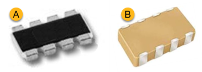
There are variations of CC resistors and capacitors that combine multiple devices into a single SMT package. They are often called arrays or networks.
In Sherlock, these are defined in a manner similar to how standard two-lead CC resistors and capacitors are defined. The main difference is seen when the number of leads increases. A four-element capacitor array, for example, has eight leads. You would still use the package dimensions provided by the datasheet, and you would follow the standard assumptions used for CC resistors and capacitors—such as assigning materials when that information is not provided by the manufacturer.