Configuring Padstacks
To configure padstacks:
- Click Home > Edit Padstacks.
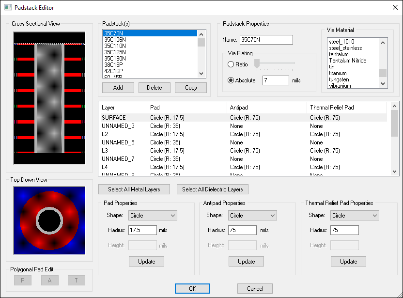
The Padstack Editor window appears.

- From the Padstack(s) area, select a padstack.
- From the layer selection box, select any metal or dielectric layer to modify the properties. If you want to apply the same properties to all metal or dielectric layers, click Select All Metal Layers or Select All Dielectric Layers.
- From the Name field, rename the padstack.
- From the Via Material list, select a material.
- From the Via Plating area, specify the thickness of the via shell using a Ratio or Absolute thickness, in mils.
The Cross-Sectional View area updates to show the vertical cross-section of the layer stackup.
To update pad properties:
- Select the layer on which you want to modify the padstack. You can also draw the padstack between two layers.
- From the Pad Properties area, use the Shape drop-down menu to select a shape for the pad, or choose None if there is no pad on that layer of the padstack. The options below will change, depending on the shape selected (e.g., if you choose a Circle, you must then choose the radius).
- Click Update to apply changes to the pad.
From the Cross-Sectional View, the innermost gray area shows the thickness of the via passing through the center of the pad. Metal colors are selected from the Edit layer properties window and the colors are proportionate to the dimensions of the pad.
To update antipad properties:
- Select the layer on which you want to modify the padstack. You can also draw the padstack between two layers.
- From the Antipad Properties area, use the Shape drop-down menu to select a shape for the pad, or choose None if there is no antipad on that layer of the padstack. The options below will change, depending on the shape selected (e.g., if you choose a Circle, you must then choose the radius).
- Click Update to apply changes to the antipad.
From the Cross-Sectional View and Top-Down view, the black area represents the antipad.
To update thermal relief pad properties:
- Select the layer on which you want to modify the padstack. You can also draw the padstack between two layers.
- From the Thermal Relief Pad Properties area, use the Shape drop-down menu to select a shape for the pad, or choose None if there is no thermal relief pad on that layer of the padstack. The options below will change, depending on the shape selected (e.g., if you choose a Circle, you must then choose the radius).
- Click Update to apply changes to the thermal relief pad.
From the Cross-Sectional View and Top-Down view, the red area represents the thermal relief pad.
From the Padstack Editor, you can also add or delete a padstack.
