
The Electronics Desktop supports importing ODB++ from many platforms. The translator relies on optional information in the EDA data file and component layer files to integrate the manufacturing data into PCB level objects such as Padstacks. If this data is missing the design may not be imported correctly. When first importing a design into Electronics Desktop, please make note of any error or warning messages; common issues include:
- Split plane layers have not been poured (generated)
- Unused interior pads are not output
- Nets have not been defined or have been "anonymized" away
- Components lack reference designators or part numbers
To access the window shown in the following diagram, refer to Importing Files into the Layout Editor. Select a .tgz file or a Windows directory to import, to open the ODB++ Import window.
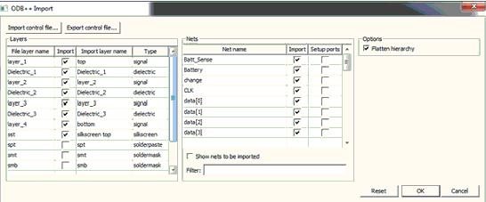
The window is initialized with the nets and layers on the imported design. Note that while signal layers can be excluded, they are imported if a hole begins or ends on that layer. Excluding layers can speed up both the translation and import into Electronics Desktop. Excluding nets can also speed up the import of a design into Electronics Desktop and make the design easier to work with.
- Import stackup and options allows you to import information from an xml control file or a layer mapping file into the window. Note the information contained in the control file is exported on the Layer Stackup window and is not directly usable by the translator if layer names are changed. One can however combine the records for renaming layers with the control file exported on the stackup window; for more information see Control File Usage with Renaming. Ansys Electronics Desktop also supports reading .tech and .layermap files.
- Export control file creates an xml control file using the information imported to the window to the location specified. This file can either be imported and used through the window or used directly with Anstranslator.exe.
Layers Pane
- Import check box specifies which layers to import. Note that while signal layers can be excluded they always be imported if the signal layer is at the top or bottom of a hole (padstack).
- Import Layer Name renames a layer. Note that all layers including drawing layers can be renamed. Once imported into Electronics Desktop this mapping are lost and you need to refer to these layers by their new name.
- Type is set based on properties in the ODB++ file and can be changed if needed.
Nets Pane
- Import check box specifies which nets to import. Ensure Dummy is checked if you want to import the metal not assigned to a specific net.
- Setup Ports automatically creates ports on the nets to be imported when checked.
Options Pane
- Flatten Hierarchy should usually be selected. This makes sure that all the component data is moved down and is ready for simulation.
Control File Usage
Importing a control file into the window preserves not only the layer settings but also the Component property section of the .xml file. This means that if you import the following control file C28 has a value of 4.7nF.
<?xml version="1.0" encoding="UTF-8" standalone="no" ?>
<c:Control xmlns:c="http://www.ansys.com/control" schemaVersion="1.0">
<Components schemaVersion="1.0">
<TypeMap>
<!-- Match C28 exactly -->
<RefDes RegEx="C28" Type="Capacitor" SC_Value="4.7n"/>
</TypeMap>
</Components>
</c:Control>
For details on the TypeMap see ODB++ Control File Part Mapping.