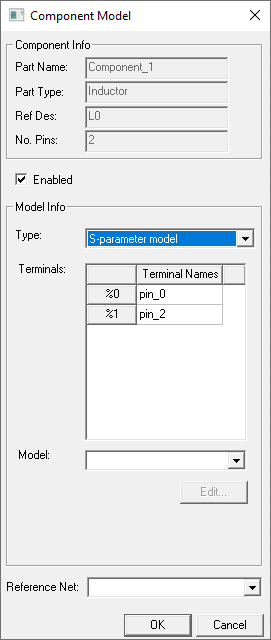
A component is a collection of entities grouped together with a common set of configurations. You can use components to configure HFSS 3D Layout objects. Complete these steps to create and edit these configurations in the Component Model window.
-
To open the Component Model window, do one of the following:
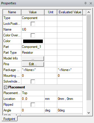
- From the Layout Editor, select a component to populate the Properties window. Then click the Model Info [...] button.
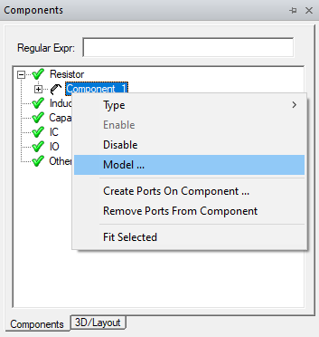
- From the Components window, right-click a component and select Model.
-
From the Component Model window, configure all the pins of a component or components of the same class. The exact configurations depend on the model type (e.g., an assigned electrical model can characterize how a passive device behaves).
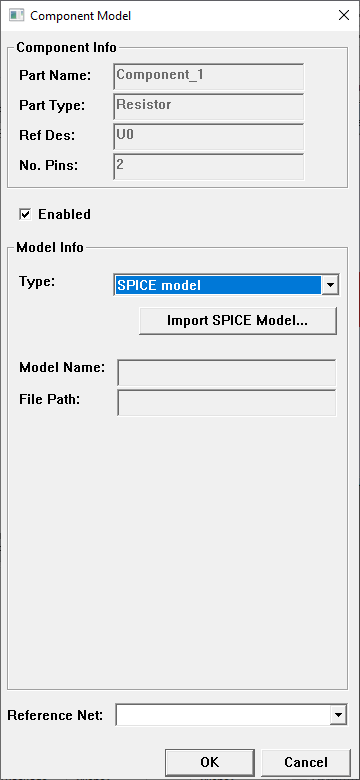
The Part Type determines what model type a component can have
|
Part Type |
Model Type |
|
Resistor Inductor Capacitor |
|
|
IC (integrated circuit) IO (input output) Other |
|
For S-Parameter and Library models, users can specify a reference net, typically, a ground/power net, to be used as reference for the terminals of the components. Whether to provide a reference net is entirely at user discretion. If no reference net is provided, one will be automatically determined.
Circuit models supersede netlist models. You can continue to edit any netlist model that exists in a legacy project or create a new circuit model with the Schematic Editor. Netlists cannot be edited in or converted to a format that can be edited in the Schematic Editor.
SPICE Model Window
You can attach a SPICE model to a specific component in the layout or to a component type. Complete these steps to attach a SPICE model to a specific component.
-
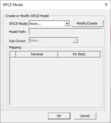
If a SPICE Model has been prepared, select it from the drop-down menu. Otherwise, click Modify/Create to open the Create/Modify SPICE Model window.
-
Enter a SPICE Model Name or accept the default (e.g., U0_model1).

-
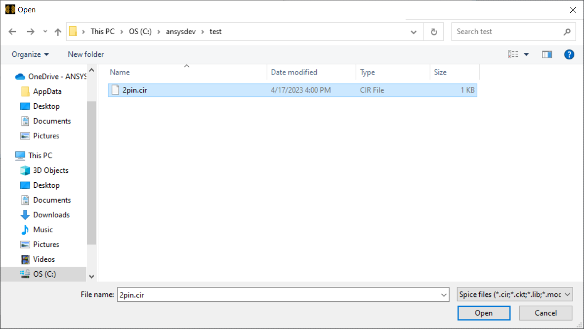
Select Create/Modify to open an explorer window.
-
Navigate to and select a Spice file (e.g., 2pin.cir). Then click Open to close to the explorer window and return to the Create/Modify SPICE Model window.
-
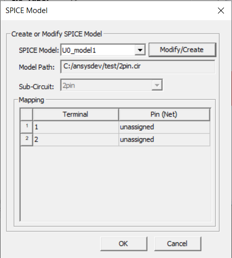
Click OK to close theCreate/Modify SPICE Model window and return to the SPICE Model window, which is now populated with the Spice file's parameters. This includes Model Path, active Sub-Circuit (if any), and the current Terminal/Pin Mapping.
-
If available, select a Sub-Circuit from the drop-down menu.
-
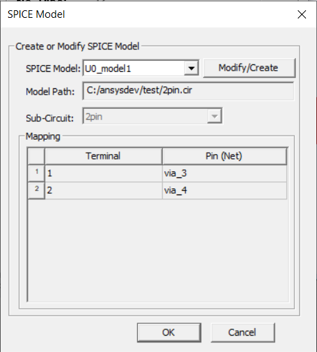
Make adjustments to Terminal/Pin Mapping by clicking in the Pin column cells and selecting a pin from the drop-down menu. Repeat, as appropriate.
-
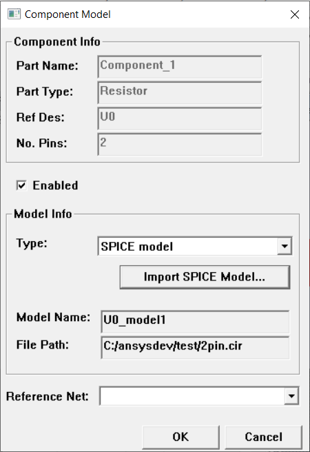
Click OK to close the SPICE Model window and return to the Component Model window. The Component Model window is now populated with the SPICE model's parameters.
Manual Model
A Manual model type contains die, solder ball, and port properties. These properties apply across the component. So, if you configure the Solder Ball Properties, every pin on the component is configured with the same type solder ball, positioned uniformly above or below, and generates a common reference for HFSS simulation.
Solder Ball and Port Properties are common for IC, IO, and other components. Die Properties are only available for IC components.
Die Properties
IC components's die properties determine the z-orientation and connections to the component’s pins on its stackup layer. There are three types of die properties: None, Flip chip, and Wire bond.
If the type is None, there is nothing connecting to the pins and no configurations to set.
With Flip chip, you configure the component’s pins to be on the top or bottom side of its layer. Chip up places the pins on the bottom side of the layer, while Chip down places them on the top side. The pins’ default depends on where in the stackup the component is.
When the Flip chip controls are available, the component’s pins connect via solder balls. So the Solder Ball Properties become available.
Wire bond type components have all pins in the same orientation, either on the top (Chip up) or bottom (Chip down) side of the layer. You can set the Height of the wires as measured on the layer.
Solder Ball Properties
When available, solder balls are identical across a component. They have the same diameters, height, and material. Solder balls can be spheroids or cylinders. Cylinders have a uniform diameter along their height.
Spheroid solder balls are spheres with the top and bottom truncated. Their Diameter is the diameter of the interface at the pin and whatever it is connecting to. The Mid Diameter is the diameter of the ball at its midpoint.
If Shape is set to None, the component does not have solder balls.
When Die Properties are available, solder balls can only be configured for Flip Chip.
Port Properties
Solder balls and wire bonds are drawn using a reference plain that is controlled by the Port Properties. By default, this plain is as large as the component and sits at the top of the solder balls and wire bonds.
The solder balls can have a Reference offset which moves the reference plane a configurable distance on the top of the solder balls.
The reference plane can be resized for solder balls and wire bonds. If Auto is enabled, the plane is the size of the component. If unavailable, set the dimension of the plane on the x- and y-axis. The plane can be as large or as small as chosen.
