Importing GDSII Format Files in IC Mode
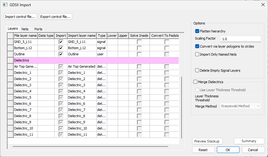
GDSII files are imported into IC Mode through the GDSII import window. This window lists layers in the design, allowing users to designate a control file (e.g., a technology definition file), select from several options, and/or import information from an XML control file, layer mapping file, or a layer filter. Once GDSII files (*.gds, *.sf, or *.strm) are imported into Electronics Desktop, they can be edited in Layout Editor (IC Mode). IC Mode reconfigures the Layout tab with new commands which will allow users to import, simplify, and convert large GDSII files into EDB (Electronic Database) files.
Importing a GDSII file
The GDSII Import window provides a basic layer mapping which is numerically ordered based on the first layers in the GDSII file. To improve the mapping, add a control or technology definition file and if possible a layer map file too. These files map layers in the GDSII file to layers in the imported stackup. Each set of geometries in the GDSII file can only appear on a single layer, so multiple file layers can map to an import layer but file layers cannot map to multiple import layers.
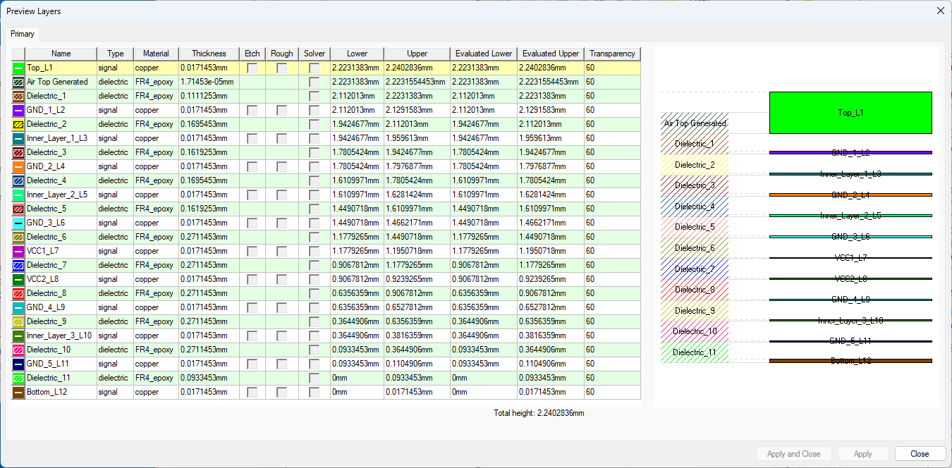
To preview the final stackup as it will appear after import is complete, click Preview Stackup.
Layers can be renamed during the import into IC Mode process, but the information contained in the control file is exported on the Layer Stackup window and is not directly usable by the translator. When a design is imported, the layer mapping is not maintained internally. To re-translate a design with renamed layers, use the same layer name that is specified in the GDSII file. It is also possible to combine the records for renaming layers with the control file exported on the stackup window. See Control File Usage with Renaming.
If all conductive layers have thickness, the three-dimensional connectivity of the design is used to generate nets. See GDSII Cell Import and Net Generation for advanced rules for importing GDSII designs.
Complete these steps to import a GDSII file with Electronics Desktop.
- From the File menu, select File > Import > GDSII to open an explorer window.
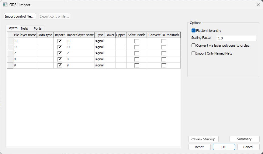
- Navigate to the chosen GDSII (.gds) file in the explorer window. Then double-click the file or select the file and click Open to open the GDSII Import window, on the Layers tab. This window contains three tabs: Layers, Nets, and Ports.
- Layers – displays layer import options, as shown previously in steps 1-2, and in steps 3-13.
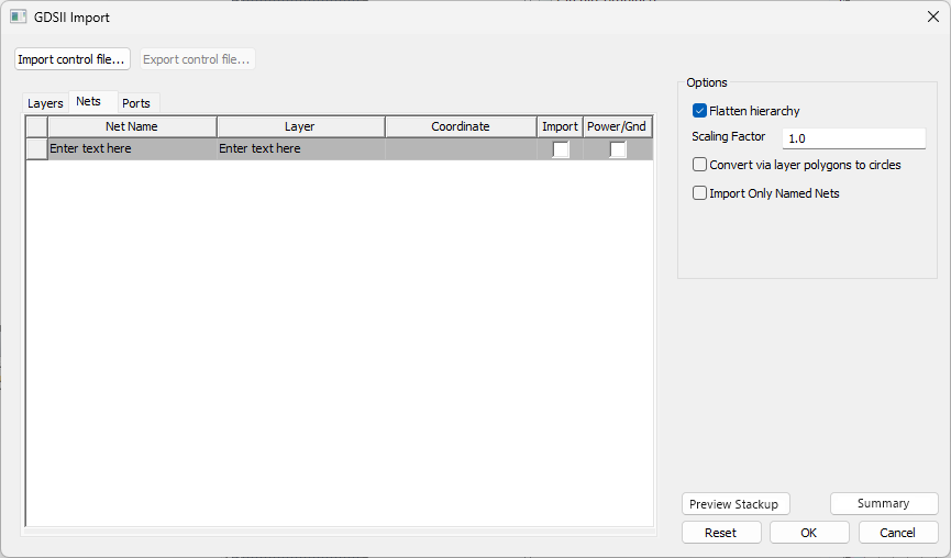
- Nets – allows users to select nets by Net Name, Layer, or Coordinate for Import and designate Power/Gnd nets.
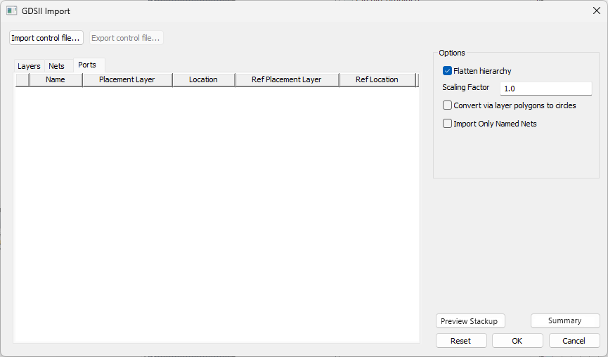
- Ports – provides a list of ports and a method of adding ports via .csv file. Refer to Add Ports From a .CSV File.
- Use an XML control file to change import settings. To import a control file or technology definition file, perform the following substeps:
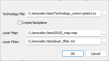
- From the GDSII Import window, click Import control file to open a window with three fields (i.e., Technology File, Layer Map, and Layer Filter).
 Note:
Note:A Technology File and Layer Map are required. All selected files must reference compatible (i.e., in sync) data or errors will result.
- Click the Technology File [...] button to open an explorer window.
- Navigate to the chosen technology definition file or control file. Then double-click the file or select the file and click Open to close the explorer window and return to the previous window.
- From the GDSII Import window, click Import control file to open a window with three fields (i.e., Technology File, Layer Map, and Layer Filter).
A technology definition file can have an .xml, .layermap, .ircx, .vlc.tech, or .itf extension.
-
If a technology definition file is imported, at user discretion, check the Create Backplane box.
- If a technology definition file is imported, click the Layer Map [...] button to open an explorer window.
- Navigate to the chosen .map file. Then double-click the file or select the file and click Open to close the explorer window and return to the previous window.
- If appropriate, click the Layer Filter [...] button to open an explorer window. A technology definition file must either contain references to the same number of signal/via layers in a design's stackup or a layer filter can be used to specify which layers from the technology definition to redefine within the stackup. Refer to Adding a Technology Definition File to a Design.
- Navigate to the chosen .txt file. Then double-click the file or select the file and click Open to close the explorer window and return to the previous window.
- Click OK to close the window and import the technology definition file and/or the map file. When an imported control file contains dielectric layers, the layers are separated in the Layers tab, and an additional Merge Dielectrics area appears beneath the Options area.
-
If appropriate, check the Merge Dielectrics area, and choose whether to utilize the Use Layer Thickness Thresholdcheck box. If the Use Layer Thickness Threshold box is checked, enter a value in the Layer Thickness Threshold field and select a Merge Method on the drop-down menu. Refer to Dielectric Simplification (Merging).
-
If appropriate, select Delete Empty Signal Layers.
- From the Layers table:
- Check the boxes in the Import column to choose which layers to import (default is all layers selected).
- Rename any layer from the fields in the Import layer name column.
- Set the type of each layer on the drop-down menus in the Type column.
 Note:
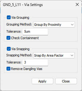
Note:If a layer's type is set to via, geometry on that layer is converted to a padstack instance between the signal layer above (Upper) and the signal layer below (Lower). Values for Upper and Lower are filled automatically. For on-chip structures, assign high-density via layers the via signal type to use the Via Grouping feature on those layers. Right-click any via layer and select Via Settings to open the Via Settings window. Make additional changes, as appropriate, then click Apply.
- If appropriate, use the check boxes for each layer to enable Solve Inside and/or Convert To Padstack.
- From the Options area, select Open With ANSYS ECAD Xplorer [Beta].
- If appropriate, enable other options in the area:
- Flatten hierarchy flattens hierarchies in a design after the design is modified in ECAD Xplorer.
- Scaling Factor scales the XY coordinates of all geometries. It does not apply to layer thickness (default is 1.0 (i.e., no change)). The scaling factor t can be any real number greater than 0.
- Convert via layer polygons to circles changes any polygons on via layers to circles.
- Import Only Named Nets only imports geometry that is assigned to a named net.
- To create a new control file that includes any changes made in this window, click Export control file...
- Click OK to open the file in ECAD Xplorer.
The procedure is complete.
The Preview Stackup Window
Click Preview Stackup to open the Preview Layers window, which displays the stackup data table and visual representation of the stackup.
The Cell Summary Window
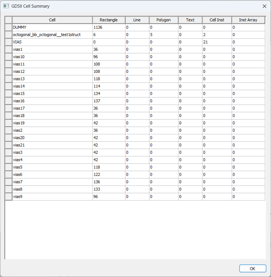
Click Summary to open the GDSII Cell Summary window, which lists the number of rectangles, lines, polygons, texts, cell instances, and instance arrays for each cell.
Adding Ports From a .CSV File
Import ports from a .csv file by following these steps.
-
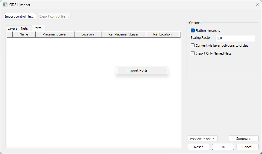
From the Ports tab, right-click in the port grid and select Import Ports to open an explorer window.
-
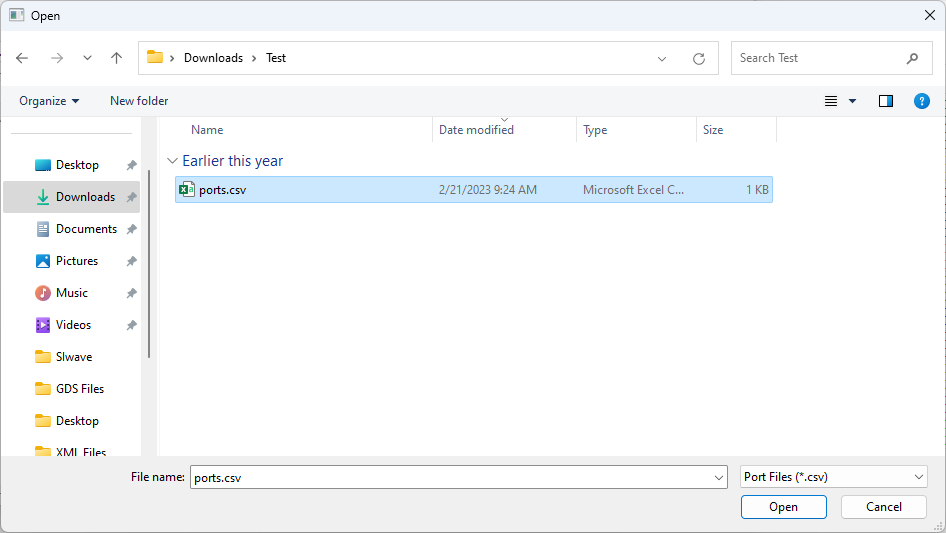
Navigate to the chosen .csv file. Then double-click the file or select the file and click Open to close the explorer window and return to the GDSII Import window.
-
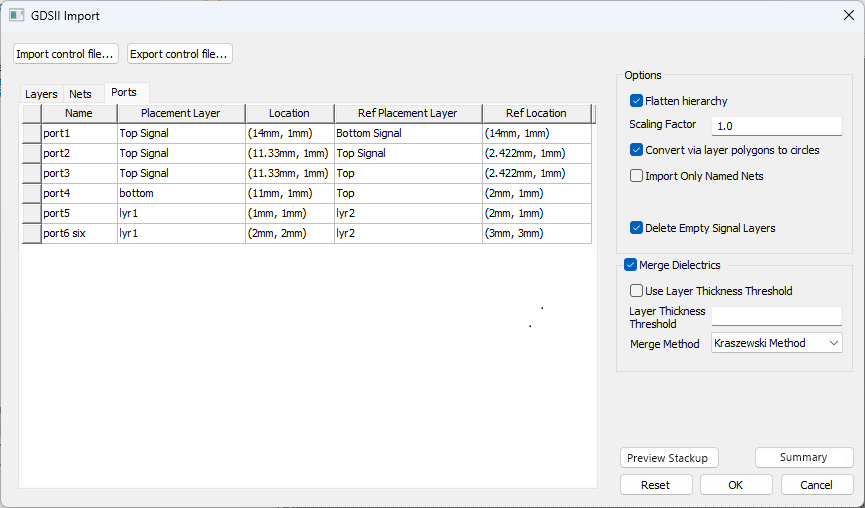
The ports grid is now populated with the data on the .csv file.
Continue to Layer Mapping and XML Control Files in IC Mode or Layout Editor (IC Mode).
