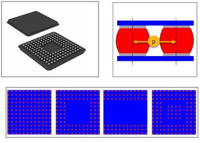
Ball Pattern: Refer to part data
sheet drawing. Ball Count: Refer to part data sheet
drawing. Ball Pitch: Refer to part data sheet
drawing. Ball Diameter: Refer to part data
sheet drawing. Ball Package Diameter: Refer to part
data sheet drawing. Ball Pad Diameter: Refer to part
data sheet drawing.
Tip: Often, data sheets do not provide Ball
Package Diameter or Pad
Diameter. As an approximation, use 90% of
the Ball Diameter.
Ball Height: Refer to part data sheet
drawing.
Tip:For Ball Height, use
max dimension, not
nominal. Datasheet dimensions for solder balls show the
geometry of the loose component before reflow with
solder paste. Add 70 to
100 μm to the stated ball
height. For larger BGAs (40 x
40 mm), the high mass of the
component will cause the solder balls to collapse
slightly, so this edit is not needed.
For Ball Grid Layout Properties (Ball Chan
Width, Ball Modeling,
Ball Perimeter Rows, Ball
Perimeter Cols, Ball Island
Rows, Ball Island Cols),
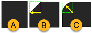
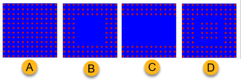
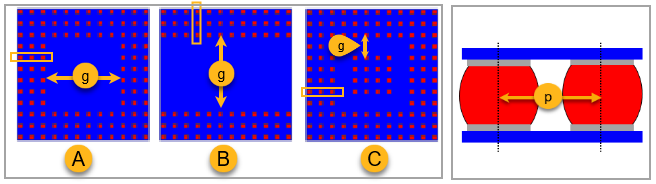
refer to the datasheet drawing, and see notes below. Ball layouts often come in standard patterns that
are defined in Sherlock: FULL
(A, below), PERIMETER (B),
CHANNEL (C), or
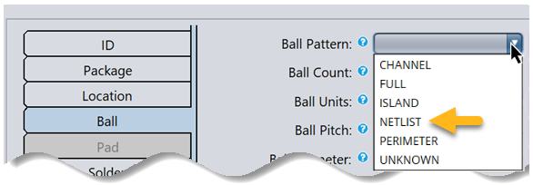
ISLAND (D). For non-standard layouts, the
NETLIST
Ball Pattern option will
extract ball location information from the PCB
design files. NETLIST will
also correctly populate ball locations for standard
grid layouts. To correctly populate Ball Chan
Width, Rows, and
Columns for standard BGA
layouts, remember: Ball Channel Width
applies only to Perimeter
(A in the image below),
Channel (B), and
Island (C) patterns.
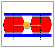
To Calculate Ball Channel
Width
| Ball Channel Width = [ball pitch] x [the
number of ball columns on one side of the
gap] |
Tip: In some cases, setting the correct ball
pattern properties can be confusing. To confirm
your work is correct, view the component in
Sherlock's 3D Viewer to verify the accuracy of the
model. See Checking Your Work.
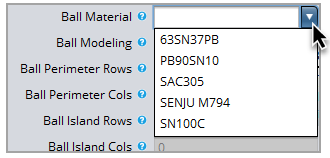
Ball Material: Refer to the part data
sheet. Ball Material is the type of
solder ball used to connect the BGA to the PCB. Supported
values are defined in the solder data file provided by
Sherlock and/or a user-defined data file.
Tip: BGA components may be assembled with solder balls
composed of a different alloy than what was selected for
the PCB solder paste.
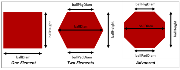
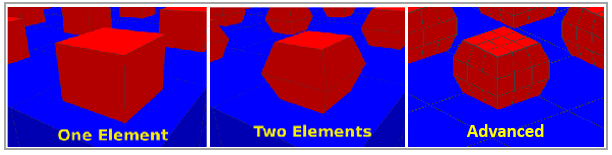
Ball Modeling:
NONE, ONE
ELEMENT, TWO ELEMENT,
or ADVANCED. For a detailed
discussion on ball modeling types, see Solder Ball Modeling in the Sherlock User's Guide.
|