
Surface Impedance Boundary Condition (SIBC) for Metal Traces of Finite Thickness
As previously noted, it is not recommended to solve inside
of conductive objects in the whole frequency range. The task is to apply
equivalent SIBC on the surface which result in the right circuit impedance
in the whole frequency range. The derivations will be detailed for internal
objects only.
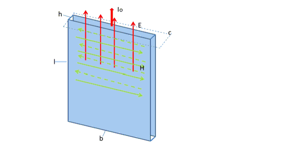
Figure 1: A conductor of finite thickness
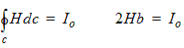
Using the notations of Figure. 1 and applying Ampere's law, we get:
|
|
|
(1) |
Integrating the Poynting vector over both sides of the object:
|
|

|
(2) |
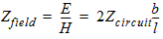
Then we get:
|
|
|
(3) |
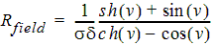
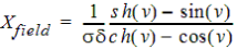
Using the circuit impedance analytical formula from [5], the real and imaginary parts of the field impedance for the SIBC are:
|
|
|
(4) |
|
|
|
(5) |
Here v=h/d and d is the skin depth. The formulas satisfy the asymptotic conditions, namely at low frequencies and

|
(6) |
|
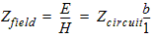
at high frequencies. For outer surfaces, where the SIBC is applied to the outer boundary of the computational domain,
|
|
|
(7) |
|
|

|
(8) |
|
|

|
(9) |
Using SIBC, the solution, including the extrapolated DC point, will be more accurate because the DC behavior is modeled accurately. Also the causality is not violated because the analytical formulas satisfy the Maxwell's equations. Experimental data shows that FEM with low frequency treatment can cope with structures when the ratio of the average mesh size and the wave length is 10-10. Assuming a PCB with 1um average mesh size. It allows us to solve down to 300 Hz.
Next