


Failure rates can be computed at SysML models based on an aggregated information from an imported IP Design (see Import of Chip Design Data (IP Design)). A higher-level block design of a chip can be created in SysML with the overall failure rates for die and package, and the distribution of the failure rate over sub-parts can be automatically derived from the implementation design using the die area, gate/cell count, or sequential element count. As precondition, allocations must exist between the SysML block level design (referred to as 'target' in the following) and an imported IP Design model (referred to as 'source' in the following).
In order to aggregate the die area, gate counts, sequential elements, etc. from an imported IP Design do the following:
Select the target scope of aggregation and choose "Prediction -> Aggregate Failure Rates..." in the context menu of the Model Browser
A wizard will open with basically two main options:
Update percentage of direct children (flat model). This option assumes that all allocations from target to the source IP design will exist at the elements directly underneath the selected element.
Update percentage based on leaf nodes (tree model). This option assumes that the selected model is mode structured than a flat list of sub-parts, so that allocations from target to the source IP design exist always at the leaf nodes.
Note that these options require a different setup of the allocations and hence depend on what has been done before executing this wizard. See also the example section below for more information.
In addition, there is an option to Exclude area/counts for children that have separate allocations. This option will essentially exclude die area/element counts in case allocations do overlap. So if the IP model hierarchy contains e.g. under an instance "i_mem" three sub-instances "i_address", "i_data", and "i_ecc", a high-level design could split the area to a "MEM" and an "ECC" block by just creating two allocations, one from "MEM" to "i_mem" and a separate from "ECC" to "i_ecc". If the option "Exclude area/counts" is used, the area and element counts of "i_ecc" will not be counted twice and only allocated to "ECC".
If allocations are inconsistent or overlap and the "exclude" option is not checked, the wizard will produce warnings for these elements on a separate page that appears now (before the summary is shown).
As a next step, the wizard will show a preview of the results. Note that you can continue with the aggregation even if the overall percentage is not 100%.
Pressing "Next" will terminate the aggregation and perform the update of the elements in the target model.
Examples
Let's assume a target model contains one "DUT" element and two children "MEM1" and "MEM2". The allocations to an imported IP design where done for "MEM1" and "MEM2", i.e. both elements have allocations to the same (or multiple) imported IP design models.
Triggering the "Aggregate failure rates..." on "DUT" makes only sense with the option "flat model", since all children are directly contained in "DUT". Since the element "DUT" was selected, the children "MEM1" and "MEM2" will be updated. In more detail, the wizard will update the prediction mode to "percentage of parent" in that target model for all directly contained parts of the selected element:
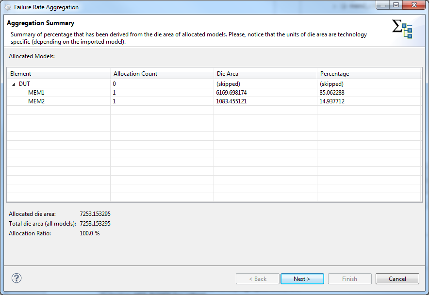
That means the failure rate associated to "DUT" can be distributed over the two elements "MEM1" and "MEM2". The wizard evaluates all allocation relationships to IP Design models and extract the die area information attached to these elements (see Import of Chip Design Data (IP Design)). Each element will receive the fraction (in percent) of the total die area.