To include a PCB in your Ansys Icepak model, click the  button in the Object creation toolbar and then click the
  button to open the Printed circuit
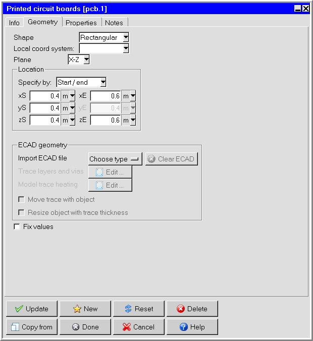
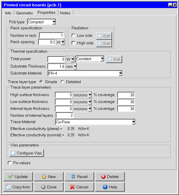
boards panel, shown in Figure 15.3: The Printed circuit boards Panel (Geometry Tab) and Figure 15.4: The Printed circuit boards Panel (Properties Tab).
button to open the Printed circuit
boards panel, shown in Figure 15.3: The Printed circuit boards Panel (Geometry Tab) and Figure 15.4: The Printed circuit boards Panel (Properties Tab).
The procedure for adding a PCB to your Ansys Icepak model is as follows:
Create a PCB. See Creating a New Object for details on creating a new object and Copying an Object for details on copying an existing object.
Change the description of the PCB, if required. See Description for details.
Change the graphical style of the PCB, if required. See Graphical Style for details.
In the Geometry tab, specify the shape, position and size of the PCB. The inputs for a rectangular object are described in Rectangular Objects and the inputs for a polygon object are described in Two-Dimensional Polygons. See Resizing an Object for details on resizing an object and Repositioning an Object for details on repositioning an object.
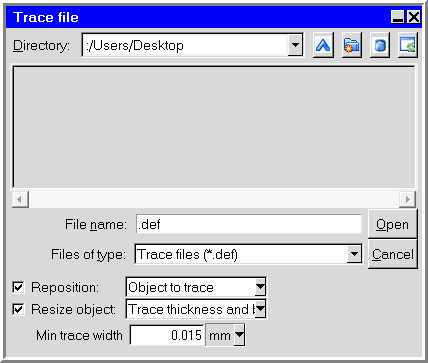
(optional) The traces and vias in the PCB can be accurately modeled by directly importing ECAD data (ODB++ EDB, ANF, or IPC2581 files). Choose ODB++ Design, Ansys EDB, Ansoft Neutral ANF, ASCII Neutral BOOL, or IPC2581 from the Import ECAD file drop-down list to display the Trace file panel. Select the associated file and click Open to import the file. After the file has been specified and imported, Ansys Icepak assigns ECAD data to the PCB and displays the trace and via information in the Board layer and via information panel. You can modify the board dimensions in the Board layer and via information panel.
The Trace file panel (Figure 15.5: PCB Trace file panel) is displayed when importing an EDB, ANF, BOOL, or IPC2581 file. Select a file and click Open to import the file.
You can modify various imported dimensions like the layer thicknesses, etc. by clicking the Trace layers and vias button (only available after importing a, anf, odb++, or IPC2581 file). You can change the values in the Board layer and via information panel. See Importing Trace Files for details.
Modeling trace heating is available for PCBs. See Trace Heating for details.
If you want to remove the BOOL, ANF, EDB, ODB++, or IPC2581 file associated with the PCB you can do so by clicking the Clear ECAD button in the Geometry tab.
In the Properties tab, specify type of PCB by selecting Compact, Detailed, or Hollow in the Pcb type drop-down list. The lower part of the panel will change depending on your selection of the Pcb type.
Define the Rack specification for the PCB. Ansys Icepak allows you to specify the number of boards in the rack of PCBs. Enter the number of boards next to Number in rack. The number of boards in the rack is 1 by default.
If you specify more than one board, you must also specify the Rack spacing between the boards. If you specify a positive value for the Rack spacing, the boards will be generated in the positive direction of the axis normal to the plane of the PCB. If you specify a negative value for the Rack spacing, the boards will be generated in the negative direction of the axis normal to the plane of the PCB. By default the spacing is set to zero.
Note: For a rack of PCBs, any power specification is applied to each individual PCB in the rack.
Specify the Radiation properties for the Low side and the High side of the PCB.
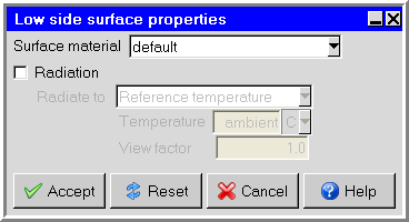
If you select Low side under Radiation in the Printed circuit boards panel (Figure 15.4: The Printed circuit boards Panel (Properties Tab)) and then click Edit, Ansys Icepak will open the Low side surface properties panel (Figure 15.6: The Low side surface properties Panel). If you select High side and then click Edit, Ansys Icepak will open the High side surface properties panel, which is identical to the Low side surface properties panel.
Specify the Material to be used for the current side of the PCB. By default, this is specified as default. This means that the material specified for the side of the PCB is defined in the Basic parameters panel (see Default Fluid, Solid, and Surface Materials). To change the material for the current side of the PCB, select a material from the Material drop-down list. See Material Properties for details on material properties.
Note: This step is not necessary for hollow PCBs because you have already performed it in step a of Board specification of Hollow PCB above.
If the side of the PCB is subject to radiative heat transfer, select Radiation. You can modify the default radiation characteristics of the PCB (for example, the view factor). See Radiation Modeling for details on radiation modeling.
Define the Board specification for the PCB.
For a Compact or a Detailed PCB:
Specify the Substrate Thickness and then specify the Substrate Material to be used for the PCB. To change the substrate material for the PCB, select a material from the Substrate Material drop-down list. See Material Properties for details on material properties.
(detailed PCB only) Specify whether you want the effective thickness of the substrate to be conserved by toggling the Conserve effective thickness option.
The trace layers are represented in the detailed PCB model using thin conducting plates. In PCBs with several metalization/trace layers, the dielectric material thickness can be significantly lower than the overall PCB thickness due to the total thickness of the metalization/trace layers. This effect will be accounted for if this option is turned on. If this option is turned off, the metalization/trace layers will not be considered when calculating the effective substrate thickness.
Specify the Heat dissipation of the boards in the rack.
For a Compact PCB, specify the Total power of the PCB to a constant value or using SIwave spatial profiles.
For SIwave spatial profiles, click Edit and select the SIwave powermap files. In the SIwave powermap profiles dialog, click Browse to select the SIwave powermap files for each layer. Click the Info button to display the contours and show the power settings of the SIwave powermap profile for each layer. Click Summary to display the Powermap summary panel, which displays information for all powermaps selected in the SIwave powermap profiles panel. Click Accept when all SIwave powermap profiles have been selected.
For a Detailed PCB, select Upper/Lower and specify the Upper face power and Lower face power of each board in the rack, or select Total and specify the Total power of the PCB.
Select Simple or Detailed for Trace layer type. If Simple is selected, specify the High surface thickness, Low surface thickness, and Internal layer thickness and then specify the % coverage for each under Trace layer parameters. Finally, specify the Number of internal layers and select the Trace Material.
If Detailed is selected, you can create additional layers by clicking the Add layer button. Specify the Layer thickness, % coverage and Layer Material for each layer under Trace layer parameters. Click Delete layer to remove the last created layer. Finally, specify the Trace Material.
The trace is the flat metal path that connects the contact sites (or pads) for the leads of components on the layer. The % coverage is the portion of the layer that is covered by traces.
For a Compact PCB, the thermal conductivity of the boards in the rack is defined to be orthogonal. The Effective conductivity (plane) and Effective conductivity (normal) are computed internally as the average of the conductivities of the substrate and the trace materials. Since the substrate thickness is greater than the combined trace layer thickness, the effective conductivity is generally much closer to the conductivity of the substrate.
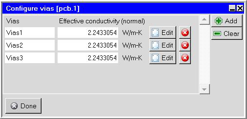
For a Compact PCB, you can edit the vias by clicking Configure Vias, which will display the Configure vias panel. Click Add to add as many vias as needed. Click Clear to remove all vias.
Click Edit to edit a row. Click the delete button (
 ) to delete a row. If you delete a row, the
rows below it shift up and are re-numbered sequentially.
) to delete a row. If you delete a row, the
rows below it shift up and are re-numbered sequentially.In the Compact Vias- Filled [Vias1] panel, select the Plane and specify the Location of the vias. Enter the following Via Details and click Accept.
Number of vias/unit Area
Via Diameter
Thickness of Electroplating
Plate material
Fill material
For a Hollow PCB:
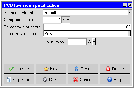
Ansys Icepak allows you to specify different physical characteristics for each side of the PCB. If you select Low side in the Printed circuit boards panel and then click Edit parameters, Ansys Icepak will open the PCB low side specification panel (Figure 15.9: The PCB low side specification Panel). If you select High side and then click Edit parameters, Ansys Icepak will open the PCB high side specification panel, which is identical to the PCB low side specification panel.
To define the physical characteristics for the low side or the high side of the PCB, follow the steps below.
Specify the Surface material to be used for the current side of the PCB. By default, this is specified as default. This means that the material specified for the side of the PCB is defined under Default surface in the Basic parameters panel (see Default Fluid, Solid, and Surface Materials). To change the material for the current side of the PCB, select a material from the Material drop-down list. See Material Properties for details on material properties.
Note: The material that you select will also be selected as the surface material in the Low side surface properties panel (see Figure 15.6: The Low side surface properties Panel).
To specify an average height for the components on the current side of the PCB, enter a value next to Component height.
Percentage of board allows you to specify the percentage of heat dissipated into the fluid from the current side of the PCB.
Specify the amount of heat dissipation from the current side of the PCB. There are three options for specifying the Thermal condition:
Select Power and enter the Total power dissipated from the current side of the board.
Select Heat flux and enter the Total heat flux dissipated from the current side of the board.
Select Per component and enter the amount of heat dissipated per component from the current side of the board. If you select this option, you can also specify the number of components as either the Total number of components or the Number per area on the current side of the board. These values are used to compute the heat dissipation for the PCB.
For an ECAD PCB:
If ECAD data are imported into the PCB, the PCB type is automatically set to ECAD. When the PCB type is ECAD, the per layer thermal properties are computed at any location using the ECAD traces (See Importing Trace Files into Ansys Icepak.
Specify the Total power of the PCB to a constant value or using SIwave spatial profiles.
For SIwave spatial profiles, click Edit and select the SIwave powermap files. In the SIwave powermap profiles dialog, click Browse to select the SIwave powermap files for each layer. Click the Info button to display the contours and show the power settings of the SIwave powermap profile for each layer. Click Summary to display the Powermap summary panel, which displays information for all powermaps selected in the SIwave powermap profiles panel. Click Accept when all SIwave powermap profiles have been selected.
![Compact Vias- Filled [Vias1]](graphics/g_ice_ug_panel_edit_vias.png)