


The simulated grain orientations do not represent crystal orientations that are typically seen in EBSD maps. This is a limitation of the current 2D microstructure model. The simulation results are good for comparing grain morphology, size and growth direction.
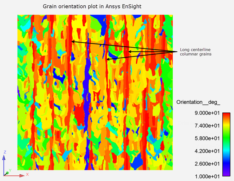
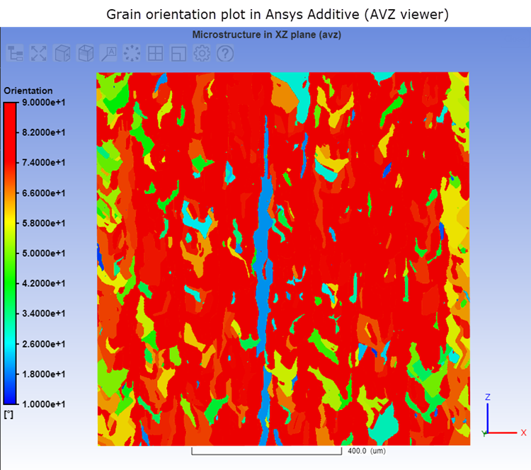
When orientation output of a Microstructure simulation is viewed in the Additive application (that is, using the AVZ viewer), the grain morphology tends to show no distinct formation. This is primarily due to the limited color scheme and data extrapolation used in the viewer. A plot of the same output, when visualized using external software, such as Ansys EnSight or Paraview, tends to show the expected grain morphology. The following figures show the same results in EnSight and with the AVZ viewer. In the first figure you can see long centerline columnar grains (marked with black arrows) that are equally separated by hatch spacing and tend to grow throughout the height of the build, along with small grains sandwiched between these long centerline columnar grains. These are typically seen in IN718 or 316L alloy when printed using a 0-90° scan pattern. This information is difficult or impossible to see when viewed using the AVZ viewer. Therefore, for best viewing purposes, we recommend using external software that allows color scheme changes, such as EnSight or Paraview, to visualize the correct grain morphology.
Certain process-parameter combinations will cause the Thermal Solver to emit a warning regarding the Mesh Resolution Factor (MRF) being too coarse to accurately resolve the maximum melt pool width. This means the element size is too large to fully capture the heat transfer phenomena in the melt pool. If this happens, increase the energy density into the system to increase melt pool width. (Currently, for Microstructure simulations, the MRF is set at 2 and you cannot change this value.)