
Computing SYZ Solutions in HFSS 3D Layout (General Mode Only)
Before starting SIwave SYZ extraction, you must define ports at the connection points for the sources and measurements, and identify the power and ground nets in your design. This is done via the SIwave Workflow Wizard's PI Configuration window.
To complete a simulation of ECAD-ECAD hierarchy (e.g., packages mounted on a PCB) or MCAD 3D components using HFSS region-based simulations, refer to SIwave Region-Based Simulations in HFSS 3D Layout.
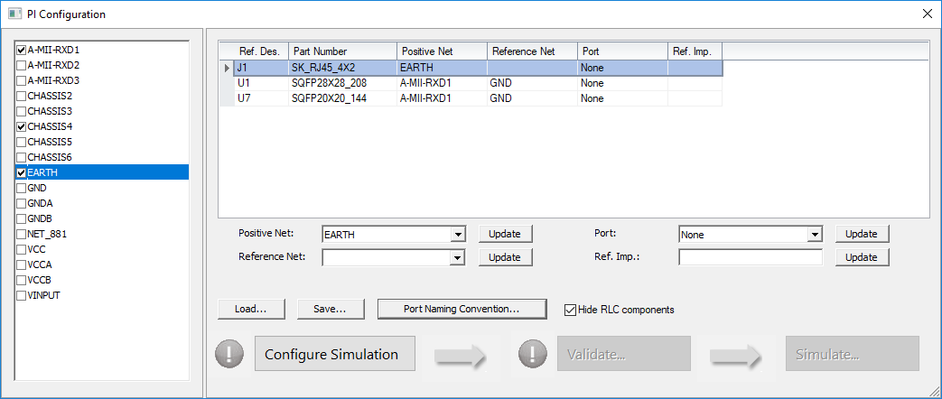
To Compute the S-,Y-, and Z-Parameters
- From the Project Manager window, right-click Analysis and select Add SIwave Solution Setup to open the SIwave Solution Setup window opens, on the General tab.
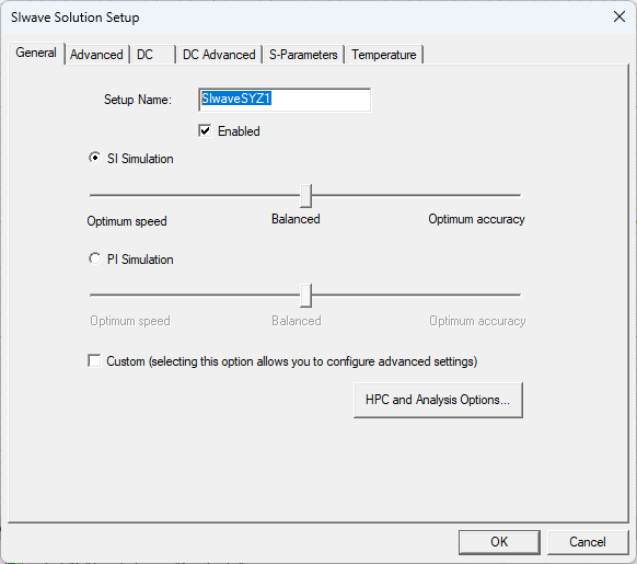
- Select either SI simulation (Signal Integrity) or PI simulation (Power Integrity), and move the corresponding slider to adjust speed and accuracy.
For SI simulations:
- Optimum speed – of the Coupling options on the Advanced tab, only Trace Coupling are selected.
- Balanced – of the Coupling options on the Advanced tab, Trace, Coplane, Split-Plane and Cavity Field Coupling are selected.
- Optimum accuracy – Trace Return Current Distribution are selected, in addition to the Balanced Coupling options.
For PI simulations:
- Optimum speed – no coupling options are selected.
- Balanced – Cavity Field coupling are selected.
- Optimum accuracy – Trace, Coplane, and Split-Plane Coupling are selected, in addition to Cavity Field.
The Custom check box allows you to configure additional options on the Advanced tab.
-
Click HPC and Analysis Options to open a window that allows you to set HPC options.
- Click the Advanced tab.
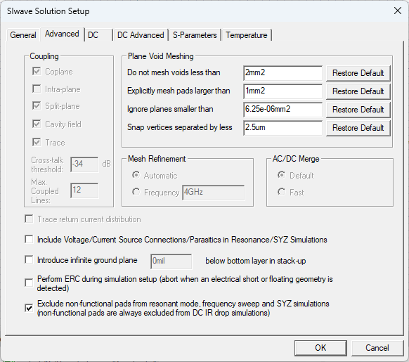
- Set the Advanced tab options:
- Coupling – selections on the General tab display and are locked. If you chose Custom on the General tab, select on the listed options.
- Plane Void Meshing – specify plane void meshing, control geometry defeaturing, and vertex snapping measurements and units, or Restore Default settings.
- Mesh Refinement – either select Automatic or specify a Frequency.
- Trace return current distribution – available only if you have selected the Custom check box in the General tab. Check this option to accurately model the change of the characteristic impedance of transmission lines caused by a discontinuous ground plane. Instead of injecting the return current of a trace into a single point on the ground plane, the return current for a high impedance trace is spread out. The trace return current is not distributed when all traces attached to a node have a characteristic impedance of less than 75 ohms, or if the difference between two connected traces is less than 25 ohms.
- Include Voltage/Current Source Connections/Parasitics in Resonance/SYZ Simulations – determine whether to include the effect of parasitic elements from voltage and current sources.
- Introduce infinite ground plane – specify the elevation of the infinite unconnected ground plane to place under the design. The ground plane serves as a voltage reference for traces and planes if they are not defined in the layout.
- Perform ERC during simulation setup – determine whether to perform error checking while generating the solver input file. In some designs, the same net may be divided into multiple nets with separate names; these nets are connected at a “star point.” To simulate these nets, error checking for DC shorts must be deactivated. All overlapping nets are internally united during simulation.
- Exclude non-functional pads from resonant mode, frequency sweep and SYZ simulations – determine whether to remove non-functional pads. All layers in which a via does not make an electrical connection to any other geometry do not contain a pad. By default, non-functional pads are not included in the simulation. Typically non-functional pads are removed when a PCB is manufactured.
- Select the DC tab.
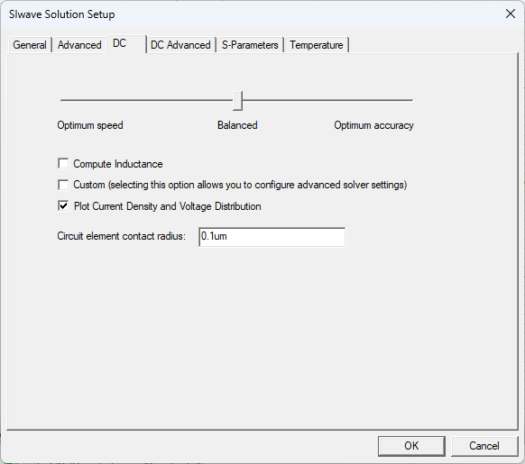
- Set the following options:
- Use the slider to balance speed and accuracy:
- Optimum Speed – all options in the DC Advanced tab are deactivated.
- Balanced – the Mesh Bondwires and Mesh Vias options are selected, along with adaptive Mesh Refinement.
- Optimum Accuracy – the mesh are refined on bondwire and vias, and more aggressive refinement parameters are specified.
- Select whether to Compute Inductance. The inductance is computed by integrating the vector potential at DC using an efficient, multi-level fast multipole method with two-level parallelization. In some cases, this may require significant computational time and memory.
- Select whether to use Custom simulation settings.
- Select whether to Plot Current Density and Voltage Distribution. Clear this check box to save disk space if you don't need to post-process voltage and current plots (e.g., if you only want to export a SPICE netlist after a DC simulation, it might not be helpful to save any field data to disk).
- Enter the Circuit Element Contact Radius. Equal potential is enforced in the contact radius, and no mesh refinement is done inside the contact region.
- Use the slider to balance speed and accuracy:
- Select the DC Advanced tab.
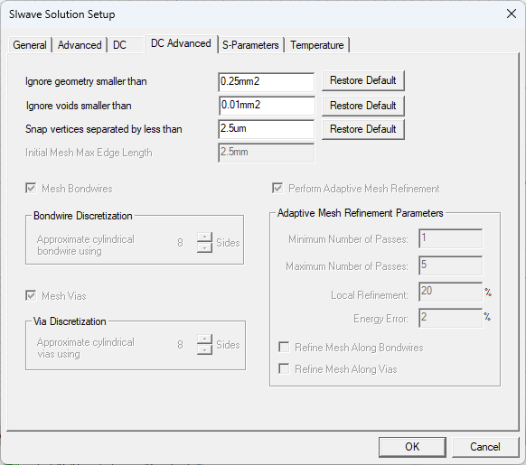
DC Advanced options include:
- Ignore geometry smaller than – geometry whose area (after being combined with any overlapping geometry) falls under this specified threshold is ignored during simulation.
- Ignore voids smaller than – geometry whose area (after being combined with any overlapping geometry) falls under this specified threshold is ignored during simulation.
- Snap vertices separated by less than – entities (e.g., vias) and vertices that are separated by less than the distance specified in this box may be snapped together during solver pre-processing.
- Initial Mesh Max. Edge Length – specifies the maximum edge length selected in the mesh (before any adaptive refinement occurs).
- Mesh Bondwires – check if users do not want to model bondwires as point connections to mesh. Specify the Bondwire Discretization (the number of sides used to approximate cylindrical bondwires). Specify any value between 6 and 64. The default value is 8.
- Mesh Vias – check if users do not want to model vias as point connections to mesh. Specify the Via Discretization (the number of sides used to approximate cylindrical vias). Specify any value between 6 and 64. The default value is 8.
- Perform Adaptive Mesh Refinement – check to perform Adaptive Mesh Refinement, and populate the fields:
- Minimum Number of Passes – an adaptive analysis does not stop unless the minimum number of passes specified has been completed, even if convergence criteria have been met.
- Maximum Number of Passes –
this value is the maximum number of mesh refinement cycles users want
the simulation to perform. This value is a stopping criterion for the adaptive
solution. If the maximum number of passes has been completed, the adaptive
analysis stops; otherwise, the adaptive analysis continues unless the
convergence criteria are reached.
Note:
The size of the finite element mesh — and the amount of memory required to generate a solution — increases with each adaptive refinement of the mesh. Setting the maximum number of passes too high can result in the Ansys Electronics Desktop (AEDT)TM electronics systems design platform requesting more memory than is available or taking excessive time to compute solutions.
- Local Refinement – this value determines how many triangles are added at each iteration of the adaptive refinement process. The triangles with the highest error is refined. The default value is 20%.
- Energy Error – the default value is 2%.
- Refine Mesh Along Bondwires – check to refine mesh along bondwires.
- Refine Mesh Along Vias – check to refine mesh along vias.
-
Select the S-Parameters tab.
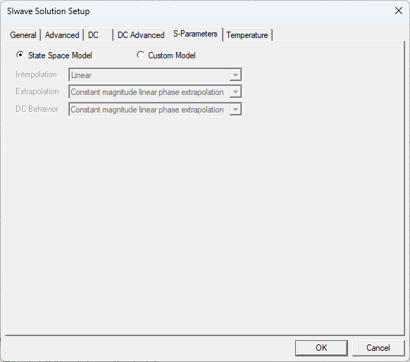
- Select State Space Model or Custom Model. If Custom Model is selected, set the following options:
- Interpolation – select Point, Linear, or Step from the drop-down menu.
- Extrapolation – select Zero padding, Same as last point, Linear extrapolation from last 2 points, or Constant magnitude linear phase extrapolation from the drop-down menu.
- DC Behavior – select Zero padding, Same as last point, Linear extrapolation from last 2 points, or Constant magnitude linear phase extrapolation, Series Capacitor, or Leave all signal lines open circuited from the drop-down menu.
Note:Refer to the following pages for an example of using the SIwave Solution Setup window to change S-Parameters or using a preconfigured Python script to generate an Ansys ECAD database file, which can then be imported into AEDT to create a custom SIwave setup.
-
Select the Temperature tab.
-
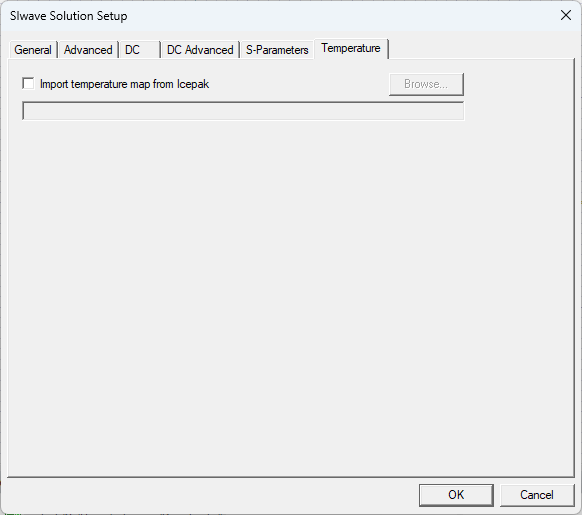
If necessary, check Import temperature map from Icepak to select either an Icepak simulation's results, or an external Ansys Icepak/Ansys SIwave temperature distribution file, then Browse to an appropriate file and select it (e.g., test.sitemp). The temperature data can locally adjust DC conductivity.
-
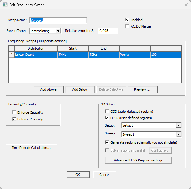
Click OK to open the Edit Frequency Sweep window.
 Note:
Note:Access this window on the Project Manager window. Expand the SIwave solution and double-click the Frequency Sweep.
- Set the following options:
- Select the type of sweep on the Sweep Type drop-down menu. Select Interpolating (default), Discrete or Broadband Fast. If you select the Interpolating or Broadband Fast sweep types, you must also specify the error tolerance (Relative error for S). An interpolating sweep estimates a frequency response for an entire range by solving a relatively small number of frequency points in the range and interpolating the remaining points.
- Choose whether to check the Enhanced AC/DC merge box to enforce causality and generate S-parameters at the DC point. By combining the DC results with the frequency-swept AC results, the simulation will have improved improve accuracy over the entire bandwidth.
Note:The following guidelines must be followed:
- You need to manually define regions. Regions must contain signal net geometry that is included in the simulation. A region containing only power/ground net geometry or signal net geometry that is not included in the simulation is invalid.
- Ports must exist either completely inside or completely outside of a region. Simulation configurations consisting of ports that straddle regions are invalid.
- HFSS regions (which are user-defined) and Q3D regions (determined by the solver) can coexist.
- Power/ground nets should be properly classified.
- Signal net geometry in the region, along with power/ground net geometry, is solved using HFSS and the resulting S-parameters are incorporated onto the SIwave solve to compute a unified channel response.
-
If present, use the check boxes in the Passivity/Causality area to enforce causality and/or passivity.
-
From the 3D Solver area, check the Q3D (auto-detected regions) box to utilize the Q3D solvers for 3D-type regions such as unreferenced traces, complex via transitions and pad coupling.
-
From the 3D Solver pane, check the HFSS (user-defined regions) box to use the predefined HFSS regions and launch the HFSS simulation options. Selecting HFSS enables options to generate a regions schematic and solve regions in parallel. These options are mutually exclusive.
Note:HFSS regions must include signal net geometry that is part of the simulation. Regions containing only power/ground nets or excluded signal nets are invalid. HFSS and Q3D regions can coexist, but ports must not straddle region boundaries.
-
If appropriate, click Advanced HFSS Regions Settings to open the Advanced HFSS Regions Settings window.
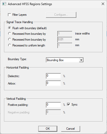
- To enable layer filtering, check the Filter Layers box. Then click Configure to open a Layer Selection window. Manually choose which signal layers are included in the HFSS region definition by checking adjacent boxes. Only selected layers will be included when defining HFSS regions. Click OK to confirm selection and close the Layer Selection window.
Note:
Filtering layers helps exclude irrelevant geometry and ensures that only signal nets intended for simulation are included in the HFSS region. Unselected layers will be excluded from simulation, and all geometry on those layers will be deleted. If all layers containing relevant signal geometry are not included, path discontinuities may result. Path discontinuity may also result if relevant GND layers are excluded (typically those immediately above and below signal layers). For example, if signal geometry exists on the Top, Bottom, and Layer 7, you should also include Layer 1 (below Top), Layer 2 (above Bottom), and Layers 6 and 8 (adjacent to Layer 7). The full set would be: Layer 1, Layer 2, Layer 6, Layer 7, Layer 8, Layer N-1, Layer N, et cetera.
- From the Signal Trace Handling area, choose how signal traces are recessed from the region boundary:
- Flush with boundary (default): Virtual ports are placed directly on the region boundary.
- Recessed from boundary by: Traces are clipped to create a gap between the virtual ports and the boundary. The recess is specified as a multiple of trace widths.
- Recessed from boundary by: Traces are clipped to create a gap between the virtual ports and the boundary. The recess is specified in millimeters.
- Recessed to uniform length: Traces are clipped so the remaining trace length is uniform across all traces in millimeters.
Note:Virtual ports must lie entirely within the region to be simulated. In the case of virtual ports generated flush to the boundary, trace routes are modified and a generous airbox is required to meet this constraint. For simulations with tight, conformal dielectric and airboxes, virtual ports must be recessed from the boundary to meet this constraint.
- From the Boundary Type drop-down menu, select the clipping method for both dielectric and airbox boundaries:
- Bounding Box: Adds horizontal and vertical padding beyond the geometry.
- Conformal: Clips exactly to the board outline (i.e., 0% padding).
- From the Horizontal Padding area, enter values for:
- Dielectric: Percentage of horizontal padding added around the dielectric region.
- Airbox: Percentage of horizontal padding added around the airbox.Note:
If Flushed with boundary (default) is selected, the boundary type is forcibly set to Bounding Box. A generous horizontal and vertical padding of approximately 15–25% is recommended. If Recessed from boundary by or Recessed to uniform length is selected, the boundary type is forcibly set to Conformal.
- From the Vertical Padding area:
- Enter values for Positive padding and Negative padding, as percentages.
- Check the Sync box to apply the same value to both directions.
Note:Vertical padding defines the extent of the simulation region above and below the board. Excessive padding may increase simulation time.
- Click OK to apply the settings or Cancel to discard changes.
-
Click OK to complete the solution setup.
-
From the Project Manager window, right-click the solution and select Analyze. The Progress window shows simulation progress. When the simulation has finished, view and export results.
Use the Advanced HFSS Regions Settings window to configure simulation boundaries and trace behavior for user-defined HFSS regions in SIwave region-based simulations. These settings affect how dielectric and airbox extents are clipped, how trace ends are recessed, and how vertical padding is applied. Refer to Ansys SIwave™ Region-Based Simulations in HFSS 3D Layout.