
Assigning Thin Conductor Boundaries in Q3D Extractor
In Q3D Extractor, you can assign a Thin Conductor boundary. See: Working with Boundaries.
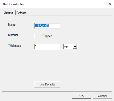
In the Thin Conductor dialog box, you are asked to specify the thin conductor Name, Material, and Thickness.
This boundary replaces a thin 3D conductor with a 2D sheet. The 2D sheet can be any curved surface without limitations.
Thin 3D conductors (aspect ratio > 1000) significantly slow down the mesh generation. This creates a problem for the solvers (ill-conditioned matrices), and results in long run times or failures. The benefits are less memory usage and shorter run times.
The solver assumes that the charges are on the 2D sheet instead of on the top, bottom, and boundary surfaces.
For example:
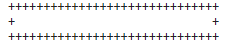
is modeled as:
++++++++++++++++++++++++++++++
where "+" are the charges.
For large aspect ratios, 3D results agree with the 2D thin conductor approach. For smaller aspect ratios, it is a tradeoff between performance and accuracy.
Capacitance and Conductance (CG) Solver
Thickness is not used by the capacitance solver.
AC Inductance and Resistance (AC IR) Solver
Like the capacitance solver, the current flows on the 2D sheet instead of on the top, bottom and boundary surfaces. For the resistance calculation, half of the surface impedance is used. This is equivalent to half of the current flowing on the top and the other half flowing on the bottom surface. The thickness is used in the inductance solver.
DC Inductance and Resistance (DC IR) Solver
The DC current flows on the 2D sheet. The thickness is used by the solver to apply the proper correction.
Assigning a Thin Conductor Boundary on a 2D Object
To assign a thin conductor boundary on a 2D object, you must select an object on the XY plane. Thin conductors can only be assigned on 2D objects (face not allowed), and you can manually assign a net on that 2D object. You can also auto identify the net, and the object will be detected as a net.