
Example Determining PCB Material Properties: Q2D and Nexxim to HFSS
This section describes the procedure for determining the PCB material properties that will be used for an HFSS simulation of a PCB.
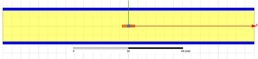
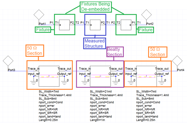
Beatty Structure
- 7 mil wide, 0.25in long 50 ohm line, with 1.4 mil thick trace and 8 mil dielectric above and below. A stripline
- 21 mil wide, 1 inch long line, with 1.4 mil thick trace and 8 mil dielectric above and below. A stripline.
Fixture is a coaxial connector with a via transition down to the stripline.
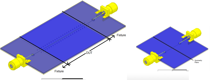
Note: The Full structure is simulated in HFSS. It is called “Measured” to illustrate that this will typically be measured data
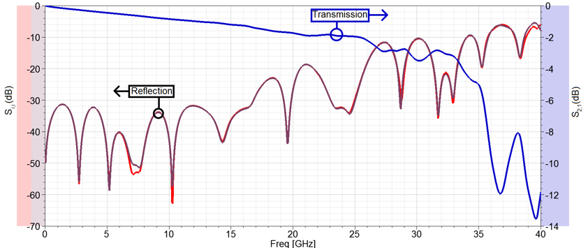
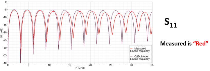
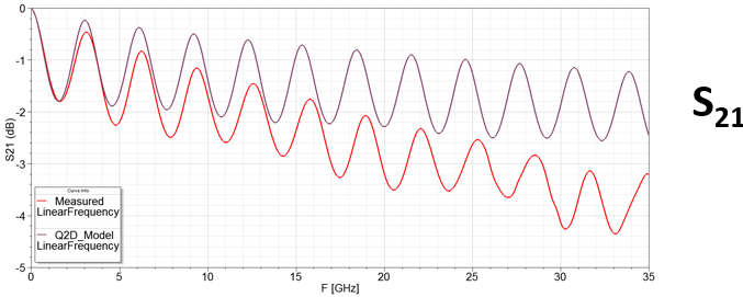
Look at 2X Thru S-parameters. There is a Good response until ~35 GHz.
- De-embedding will be questionable above this frequency
- Still good for the “lower” frequency data.
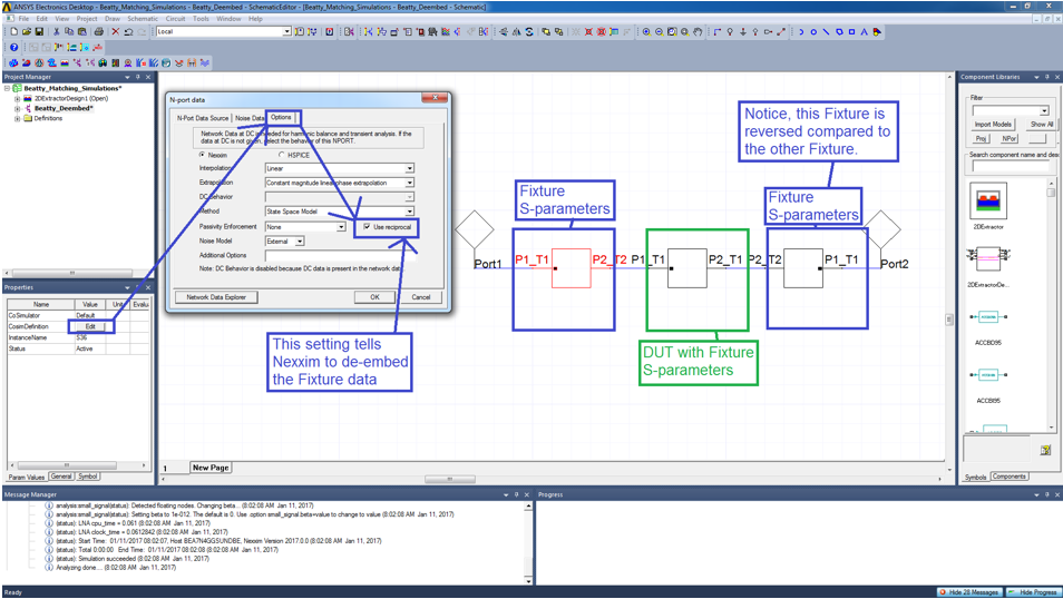
De-embed in Nexxim
- Get Fixture S-parameters using Automatic Fixture Removal (AFR as described in Reference [5]).
- Cascade Fixture S-parameter block (with reciprocal turned on) with measured data to get just the Design Under Test (DUT).
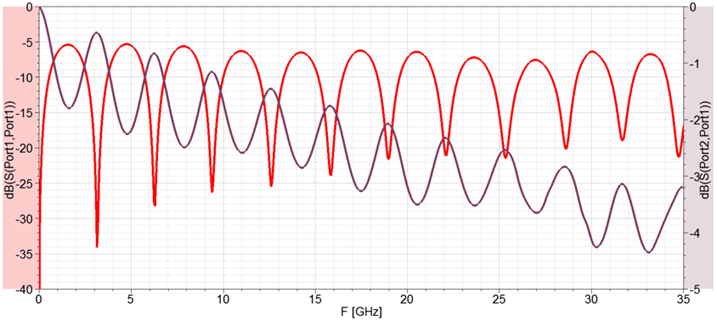
De-embedded Results in Nexxim. We clearly see the resonances
Q2D Model
Now make Q2D model of the transmission lines and perform circuit simulations with Nexxim
Fully Parameterized so we can optimize response to extract material properties.
- Width, thickness
- Metal conductivity and surface roughness: Roughness assumed the same on top/bottom of trace and on two GND planes
- Dielectric constant and loss tangent.
Fix the following because they were measured:
- Line width is 7 mils (for 50 Ω sections) and 21 mils for Beatty Section
- Metals are all 1.4 mils thick
- Total substrate thickness (from Top GND to Bottom GND) is 17.4 mils.
Nexxim with Q2D Model
Run the Q2D model in Nexxim with the following to compare to our measured results.
- Copper Conductivity = 5.8x10⁷ S/m
- Dielectric Constant = 3.66
- Loss Tangent = 0.004
- Hall-Huray Nodule Radius = 0.4 um
- Hall-Huray Surface Ratio = 1.9
Nexxim Model Results
Notice the Q2D model does not match
In Nexxim, you need to make εr lower so that the maxima/minima are further apart
Nexxim Model with Changed εr
Use Optimetrics to automatically sweep εr. Notice εr =3.48 is best.
Now look at DC Resistance
Nexxim Model, Changing Conductivity
Use Optimetrics to automatically sweep Conductivity.
Notice is closest 5.0x10⁷ S/m. This has very little impact on results.
|
Observations So Far
- We have determined εr =3.48 and conductivity of the metal is 5.0x10⁷ S/m
- Add more roughness to make loss match in lower part of band.
- Use Optimetrics to automatically sweep Nodule Radius and Surface Ratio
- Nodule Radius = 0.5um and Surface Ratio = 2.9 appears to be best fit.
Change Loss Tangent
Use Optimetrics to automatically sweep Loss Tangent.
Loss Tangent = 0.008 appears to be best fit at high frequency.
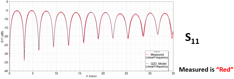
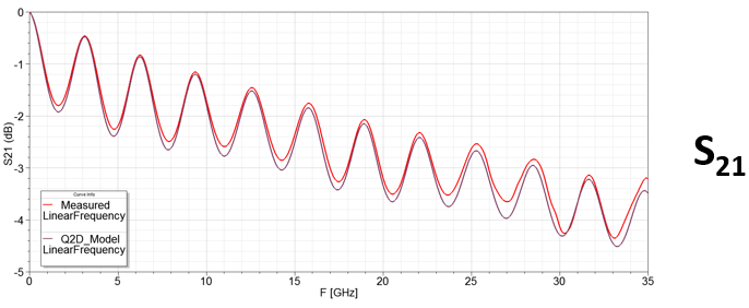
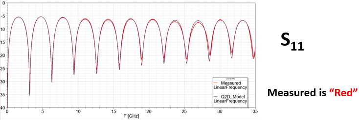
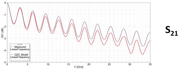
Final Values from Nexxim and Q2D
The final tuning gives:
- Copper Conductivity = 5.0x10⁷ S/m
- Dielectric Constant = 3.48
- Loss Tangent = 0.008
- Hall-Huray Nodule Radius = 0.5 um
- Hall-Huray Surface Ratio = 2.9
You can use Optimizer to match S-parameters as well. The goal of this example is show how each parameter changes the response in order to build your intuition in using them.
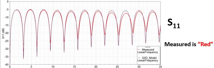
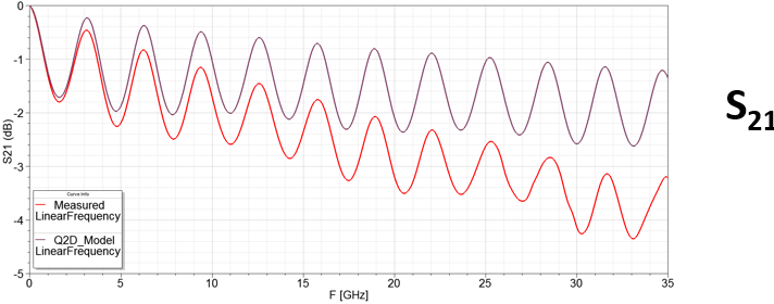
Compare HFSS Simulation with Extracted Parameters
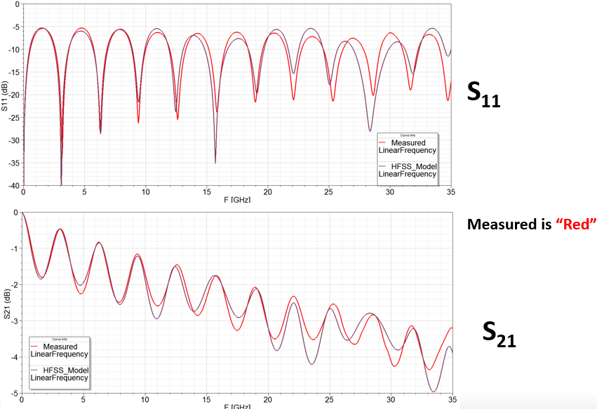
Final Tuning Values
- Copper Conductivity = 5.0x10⁷ S/m
- Dielectric Constant = 3.48
- Loss Tangent = 0.008
- Hall-Huray Nodule Radius = 0.5 um
- Hall-Huray Surface Ratio = 2.9
Summary of the Method for using Nexxim and Q2D to Determine PCB Parameters for HFSS
- Use the Beatty Standard to characterize loss
- Use proper calibration, or de-embedding, to get to actual structure.
- Use Q2D with Nexxim
- Deembed using Nexxim
- Quickly (in seconds) simulate variations of line to match measured data
- Validate extraction with HFSS simulations
- Ideally have multiple structures to measure and simulate to verify parameters.