
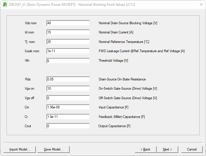
Nominal Working Point Values for Power MOSFETs
|
Nominal Drain-Source Blocking Voltage [V] |
Listed as VDD in the test conditions area of the switching characteristics section of the datasheet. |
|
Nominal Drain Current [A] |
Listed as ID in the test conditions area of the switching characteristics section of the datasheet. |
|
Nominal Reference Temperature [oC] |
This will generally be listed as Tc for the maximum temperature test conditions for the switching characteristics. |
| FWD leakage current under Nominal Conditions [A] | This value should remain at the default value unless specified in the manufacturer’s specification. This parameter directly set the FWD leakage current in the extracted device model. It has little influence to static or dynamic fitting of the model. |
| Threshold Voltage [V] | Listed in table of characteristics. |
| Drain-Source On-state Resistance [Ohm] | Listed in datasheet as RDS(on) in table of characteristics |
| On-Switch Gate-Source (Drive) Voltage [V] | Listed as Vge in the switching characteristics test conditions. |
| Off-Switch Gate- Source (Drive) Voltage [V] | This parameter may be listed in the switching characteristics test conditions; however, it often is not. A rule of thumb is to use the negative of the Vge(On) value above. |
| Input Capacitance [F] | Listed in table of characteristics. |
| Feedback Capacitance [F] | Also known as reverse transfer capacitance or Miller capacitance. Listed in table of characteristics. |
| Output Capacitance [F] | Listed in table of characteristics. |
When finished, click Next to continue characterizing the device (See Breakthrough Values).