Selecting PSI Simulation Options
Some PSI parameters can be set globally for all simulation types. These global parameters include geometry options, solver settings, and mesh refinement settings.
To define the global PSI options in SIwave:
- Click Simulation.
- From the PSI area, click Options.
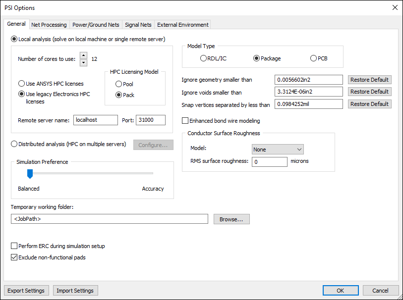
- Use the radio buttons to select either Local analysis or Distributed analysis. Options will gray out or become visible accordingly.
Note:
The option to choose a license type (either Ansys HPC or Electronics HPC) is not available when SIwave is running in Pro/Premium/Enterprise licensing mode.
- For Local analysis, set the number of cores to use, licensing options, and remote server preferences.
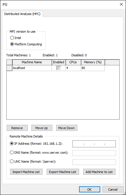
- For Distributed analysis, click Configure to set licensing and remote server preferences:
- Use the Simulation Preference slider to balance the simulation toward accuracy or speed.
- From the Model Type area, use the radio buttons to select RDL/IC, Package, or PCB. Based on your selection, simulation parameters, such as meshing and polygon defeaturing, are automatically tuned for optimal robustness and performance.
- Specify the location of the Temporary Working Folder. To specify a temporary working folder other than the default job path, click <JobPath>, and enter the location, or click Browse.
- If appropriate, check the boxes for additional options:
- Ignore geometry smaller than – geometry whose area (after being combined with any overlapping geometry) falls below this specified threshold is ignored during simulation.
- Ignore voids smaller than – voids whose area (after being combined with any overlapping geometry) falls below this specified threshold is ignored during simulation.
Note:
Ansys recommends using the default settings. Refer to Advanced Geometry Processing Options.
- Snap vertices separated by less than – entities (e.g., vias) and vertices that are separated by less than the distance specified in this box may be snapped together during solver pre-processing.
- Enhanced bond wire modeling – models wire bonds with greater definition (this also increases run time and memory requirements).
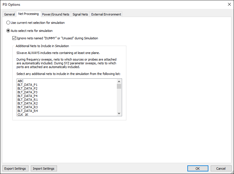
- Ignore nets named "DUMMY" or "Unused" during Simulation – uncheck this to include dummy/unused nets in the simulations. By default, all such nets are ignored.
- Perform ERC during simulation setup – use to turn error checking on or off while generating the solver input file.
- Exclude non-functional pads – remove non-functional pads. All layers in which a via does not make an electrical connection to any other geometry do not contain a pad. By default, non-functional pads are not included in the simulation. Typically non-functional pads are removed when a PCB is manufactured.
In some designs, the same net may be divided into multiple nets with separate names - these nets are connected at a star point. To simulate these nets, the error checking for DC shorts needs to be turned off, and all overlapping nets are internally united during simulation.
- Specify the Conductor Surface Roughness options for a better-refined conductivity calculation. See RMS Surface Roughness and Conductivity Technical Notes.
- Select the Net Processing tab.
- Use the radio buttons and list to select nets to include in your simulation.
- Select the Power/Ground Nets tab.
- Use the Improved loss model drop-down menu to select a model.
- From the Ignore Small Holes area, use the radio buttons to either automatically detect small holes or specify the diameter that constitutes "small." Anything below that value will be ignored.
- Select the Signal Nets tab.
- Use the Error tolerance drop-down menu to specify a value. This value is normalized to one for performing the dynamic analysis computations. The smaller the error tolerance value, the more accurate (and longer) the computation. By default, the error tolerance setting is tied to the speed-balance-accuracy slide setting: A value of 0.02 is tied to Accuracy, and 0.04 is tied to Balanced.
- Use the Conductor modeling drop-down menu to select either Mesh inside or Impedance boundary.
- Check the Improved metal loss handling check box to improve the accuracy of frequency dependent metal loss due to skin-effect.
- Check the Improved dielectric fill refinement in metal layers check box to control accuracy. However, increasing the accuracy also substantially increases the simulation time by as much as 50%. Ansys recommends leaving this option unchecked because the default setting provides sufficiently good accuracy and faster simulation.
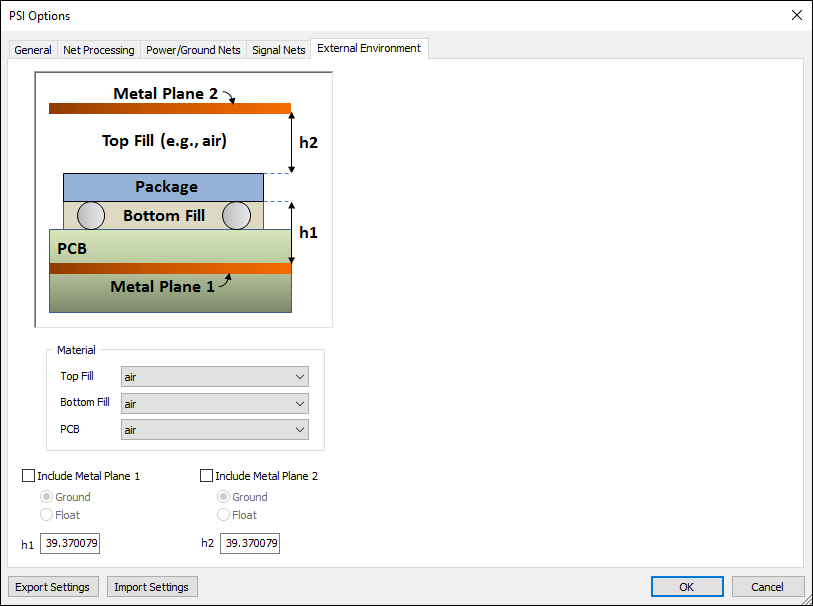
- Select the External Environment tab.
- From the Material area, use the Top Fill, Bottom Fill, and PCB drop-down menus to select materials.
- Check Include Metal Plane 1 and Include Metal Plane 2 to add up to two metal planes to the model. Metal Plane 1 represents the upper PCB Ground or VDD plane. Metal Plane 2 can represent a metal cover, a heat sink, or any other metal plane located above the package. This metal plane behaves similarly to Metal Plane 1.
- For each selected metal plane, select either Ground or Float.
- Select Ground to use the metal plane as part of the return path. This configuration affects the inductance and capacitance of the package nets.
- Select Float to leave the metal plane floating. This configuration affects only the capacitance of the package nets.
- For each selected metal plane, enter a value for height:
- h1 represents the distance from the bottom layer of the package stackup to the top of Metal Plane 1. The solder balls included in this space add to the inductance and capacitance effects on the package nets.
- h2 represents the distance from the top layer of the package stackup to the bottom of Metal Plane 2.
- Optionally, use the Export Settings button to save your settings as an SIwave Sim Settings File (*.sws). Click Import Settings to browse and select an *.sws file for import.
- Click OK to apply all settings.
The PSI Options window appears, on the General tab.
Temporary working files are created during analysis. These are later deleted after the analysis completes. If the job path points to the local computer, but the analysis was run on a separate server computer, then the temporary working files would transfer across the network to the local computer, thereby slowing down the simulation. Therefore, to improve the simulation run time, ensure that the analysis stores these temporary files on the computer running the application and not over the network.
This option applies only when Conductor modeling is set to Impedance boundary in the Signal Nets tab of the Simulation Control window. In this case, the surface boundary condition is used and a finite-element mesh is not generated inside the metal conductor. Using the boundary condition models causes the frequency sweep to converge more slowly and increases run time.
The Net Processing tab displays.
The Power/Ground Nets tab displays.
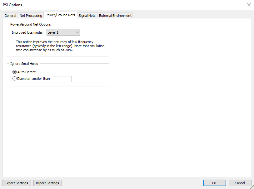
To measure metal loss in power and ground nets with greater accuracy at low frequency, typically in the kHz range, you can apply additional levels of complexity in the loss model. Ansys recommends using Level 1because the higher-order loss models substantially increase run time. For signal simulations that need higher accuracy, Level 2 should suffice.
The Signal Nets tab displays.
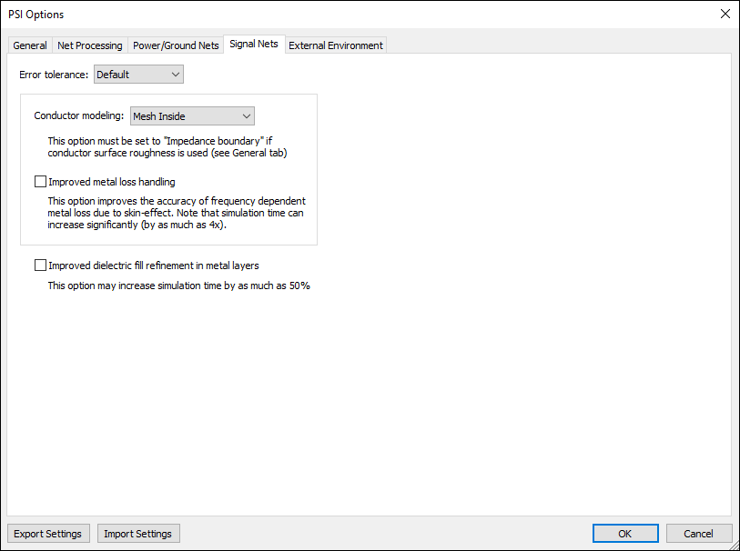
If you selected one of the conductor surface models in the General tab, you must use the Impedance boundary option.
The External Environment tab displays.
