
Specifying Chip Package Protocol Header Information in Q3D Extractor
Chip Package Protocol (CPP) is a set of statements specifying the location, the net information, and the SPICE node name for each package pin (the landing pad of flip-chip bumps or the chip landing pad of bonding-wires). It is embedded within a SPICE-compatible file header as comments.
The CPP is primarily used to help automate the co-simulation of IC (die) and package or package/board. For example, Apache's Redhawk utilizes CPP to import the package or package and PCB model into the full chip dynamic voltage drop analysis, and the global IO-SSO analysis. Package/PCB simulation tool can utilize the CPP to import the chip model in the system level analysis.
To specify the CPP information:
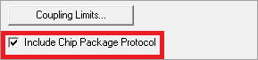
- When exporting circuit data, select the Include Chip Package Protocol check box.
- Click Edit.
The Edit Chip Package Protocol window appears.

- Set the following options:
- Package Type – Choose from wirebond dieup, wirebond diedown, flipchip dieup, and flipchip diedown.
- Coordinate System – Select either Global or a custom coordinate system.
- Length Units – Select the unit of measure.
- Use the options under Set Pins Attributes to select pins.
- Select pins by – Use the drop-down menu to sort pins by component name, pin name (number), pin type (signal or power ground), net name, or port type (DIE, PCB, VRM, OTHER). Enter a regular expression into the search field and click Select to select the applicable pins.
- Select All – Click to select all pins in the design.
- Use the Component Name, Pin Type, and Port Type fields to modify the information for selected pin(s). Click Set to apply changes.
- Click OK to exit the Edit Chip Package Protocol window.