
Trace Mapping [Beta]
In Mechanical designs, Trace Mapping is a beta feature supported for the following solution types:
- Steady-State Thermal
- Transient Thermal
- Structural
You do not have to enable any beta option to expose the trace mapping feature; it is always available for the supported solution types.
This feature and the underlying Layout Component functionality it uses are always enabled. That is, there is no beta option that you need to select in the general options to expose the functionality.
Trace Mapping is a means of accounting for the electrically conductive, and structurally stiffer, traces of a printed circuit board (PCB), including pads, vias, and conductor pour areas without actually including the conductor geometry in the mechanical design. To perform trace mapping, use a previously created HFSS 3D Layout design of a PCB as a source for a Layout Component in your Mechanical design. The conducting objects are visualized in the mechanical layout component, but they are not directly included as 3D geometry. The solved geometry consists only of the dielectric layer material (such as FR4) and the dielectric fill material specified for signal layers. However, the conductors are accounted for by locally modifying the material properties (thermal conductivity, density, and specific heat for thermal solutions; Young's modulus, Poisson's Ratio, density, and thermal expansion coefficient for structural solutions). The History Tree lists the source layout component's conducting and dielectric layers and their materials, not the material properties used in the mechanical design.
The fill material for signal layers is specified in the Edit Layers window of the source HFSS 3D Layout design. Though this fill material is not listed in the History tree of the Mechanical design, it is used in the soulution of the layout component.
Similarly, the via plating material is specified in the Edit Padstack Definition dialog box of the source HFSS 3D Layout design. If "None" is specified, the plating material is taken from the first (topmost) signal layer of the layout. The plating material is not listed in the History tree of the Mechanical design, but it is used in the layout component solution.
For structural solutions, solid dielectric material properties are substituted for air. Gases and fluids cannot support structural boundary conditions. The substitution ensures that these layers are able to support force and pressure excitations or fixed support and frictionless support boundaries.
In HFSS 3D Layout designs, cutouts and via holes are voids and are not meshed. As such, no fill material specification exists in the source design for these items. For thermal solutions, you define these materials as part of the layout component definition. Air is the default fill material for cutouts, and copper is the default fill material for via holes. For structural solutions, cutouts are handled as non-solve-inside objects. These objects exist but are not meshed, representing voids in the model, similar to the source HFSS 3D Layout design. Therefore, the cutout fill material option is not applicable to structural solutions and does not appear when defining a structural layout component.
The signal layers exists in the mechanical design as a contiguous volume of the layer's dielectric fill material. The solver modifies the fill material's properties locally, element-by-element, based on a metal fraction map, which is derived from the source layout's conductor geometry. The resolution of the metal fraction map is user-defined and needs to be fine enough to accurately capture the metal distribution on the board's signal layers. Metal fraction values are also mapped along the full length of vias, through dielectric and signal layers. See Technical Notes: Metal Fraction Map for more details.
Significance of the metal fraction map resolution: You define the number of columns and rows into which the board's length (X dimension) and width or height (Y-dimension) are to be divided. You can specify the resolution numerically or using a slider. Each cell in the resulting grid is assigned a value between 0 and 1, inclusively. The numbers represent the decimal portion of each cell that consists of conducting metal. For example, a value of 0.45 indicates that 45 percent of the cell is metal and therefore, 55 percent is dielectric. The thermal or structural material properties of all elements will be somewhere between the dielectric/fill material and the conductor material, inclusively. When an element extends into two or more grid cells, the element's metal fraction value is interpolated, and the material properties are based on the interpolated metal fraction value.
- A general guideline for good results is to set the number of columns and rows such that the cell width and height are about half of the narrowest trace width or half of the smallest via diameter, whichever result is smaller. For example, assume you have a 200 mm x 100 mm PCB with a minimum trace width of 0.5 mm and a minimum via diameter of 0.8 mm. Since the minimum trace width is less than the minimum via diameter, trace width controls the grid resolution. For a target resolution of 0.25 mm (half the trace width), the number of columns and rows would be 800 (200 mm / 0.25 mm) and 400 (100 mm / 0.25 mm), respectively. A finer resolution (more columns and rows), though it might slightly further improve the results, should not be necessary. There is a diminishing return as the grid is made finer and a significant increase in solution time and storage requirements.
- The material property mapping for layout components is mesh-sensitive. The number of elements in the X and Y directions should be no fewer than one-fourth of the specified number of columns and rows in the grid. For the example just given, the recommended minimum number of elements along the X and Y directions would be 200 (800 / 4) and 100 (400 / 4), respectively.
- To ensure an adequate mesh density, assign a length-based mesh operation to all layers of the layout component. Specify a maximum length of three to four times the smaller of the grid cell width or height.
There are several ways to create a layout component in a Mechanical design:
- Select an existing Ansys ECAD Database (*.aedb) folder previously created by, or imported into, HFSS 3D Layout.
- Any layout component that already exists in the current project's Component Library (under Definitions > Components in the Project Manager) also appears in the Definition drop-down menu when adding a new component. Pick the listed name to add a second instance of the component or to re-add a previously deleted component.
- Select a layout component file (*.aedbcomp) previously exported from an HFSS 3D Layout design.
Heat Sources
You can define heat sources for steady-state or transient thermal solutions in any combination of the following three ways:
- Specify the Power Dissipated in the layout component definition:
- Add solid objects on the PCB faces and assign Heat Generation to them:
- Overlay shell objects on the top or bottom PCB face and use these objects to assign Heat Flux excitations at selected areas:
This method distributes the specified power uniformly throughout the PCB volume. It is a convenient way to account for the heat input of many small circuit components mounted all over the PCB without having to individually include the components and their heat generation excitations.
This method localizes the primary heat sources and also can account for convective heat dissipation from the faces of the mounted components. Currently, this is the best way to account for major heat contributors, such as integrated circuits and power transistors, since the capability of importing components from the source layout is not yet implemented for layout components in mechanical desings.
If you specify convection at the PCB faces in the layout component definition, the area under any adjacent solid objects you add to the board will be filtered out of the convection boundary. This is the desired behavior since the board surface under the mounted electronic parts is not exposed to the ambient air. Select exposed faces of the components you add and assign convection to them.
Like the second method, this one localizes the primary heat sources. Heat flux at a shell object can represent the heat conducted to the PCB from a component, or a group of components, without including additional solid geometry.
You cannot imprint faces of a layout component to split them into subfaces for the purpose of localized boundaries or excitations. To perform imprinting, if it were supported, you would have to draw an object anyway. So, as an alternative to adding solid parts, you can draw shells overlaid on the top or bottom PCB face for localized boundaries or excitations. Keep the default infinitesimal thickness of the shell object (1e-7 mm) so that the shell doesn't provide a significant parallel heat conduction path. Alternatively, set the shell thickness and material to approximate the thermal conductivity of the mounted component(s) it represents.
Additionally, if you specify convection at the PCB faces in the layout component definition, do not also assign convection to overlaid shells. Convection boundary areas are not automatically filtered out at shell-to-solid object intersections as they are for solid-to-solid intersections. Assigning convection to the board face and the shell would exaggerate convective heat loss by providing a parallel and redundant heat dissipation path.
You cannot assign boundaries or excitations to layout components in the same way as you do for general objects or faces. That is, you cannot select the layout component or its faces in the Modeler window and execute a boundary or excitation assignment command.
Thermal Boundaries
Two thermal boundaries are supported, and you can assign these to the top or bottom face of the PCB only as part of the layout component definition. Specifically, the following boundaries are supported. You can assign only one of these boundaries at a time to a given face; they are mutually exclusive:
- Convection
- Temperature
For layout component (LC) top and bottom faces, you can optionally include radiation effects when defining a convection boundary, regardless of whether you select the Non-Uniform film coefficient option. This capability differs from convection boundaries assigned to general objects or faces, which can only indirectly represent radiation when importing non-uniform coefficients from an Icepak solution in which radiation was enabled.
When choosing to import Non-Uniform film coefficients from Icepak, and if radiation was enabled in the source Icepak solution setup, do not enable radiation in the Mechanical LC definition. Doing so would cause redundant radiation effects to be included in the solution, exaggerating the radiative effect. However, if the Icepak setup did not have radiation enabled, you can enable it in the target Mechanical LC definition to account for radiative heat transfer in addition to the convective transfer.
Thermal excitations are not supported for layout components with the exception of a total dissipated power that you optionally can specify as part of the layout component definition. Assign excitations, such as Heat Generation, to objects added to the model (for example, discrete semiconductors, integrated circuits, passive components, or power transformers mounted to the surface of the PCB).
Structural Boundaries and Excitations
There are two structural boundaries and two structural excitations supported for layout components, and you can assign these to the top or bottom face of the PCB only as part of the layout component definition. You can assign only one of these boundaries or excitations at a time to a given face; they are mutually exclusive:
- Boundaries:
- Fixed Support
- Frictionless Support
- Excitations:
- Force
- Pressure
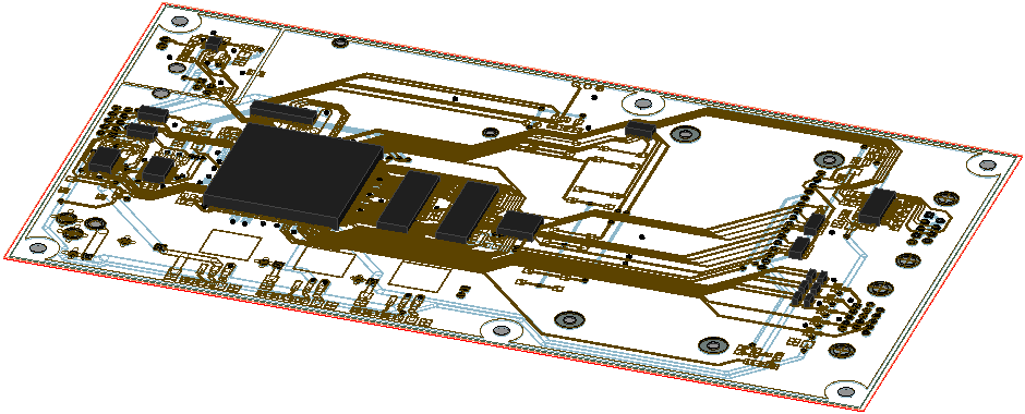
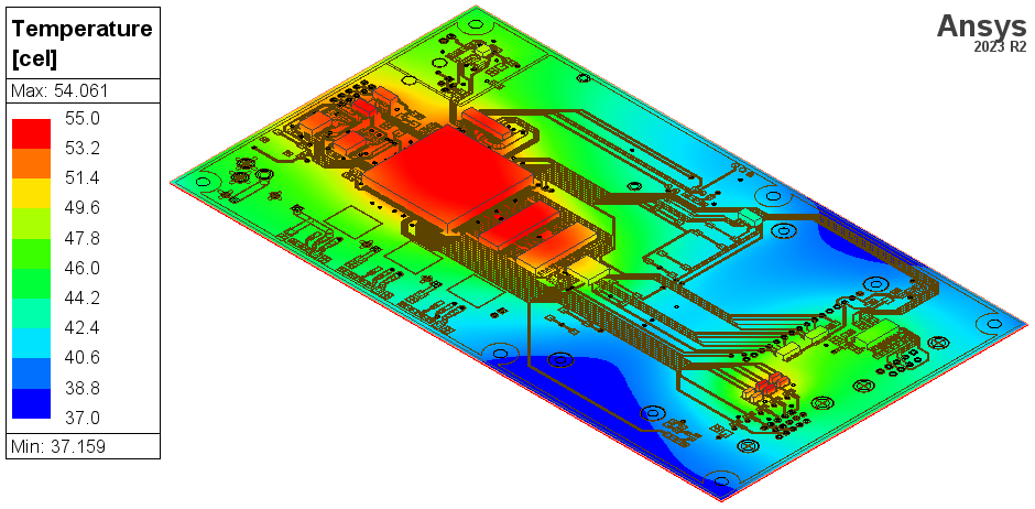
Example
The following figure is a PCB layout component in a mechanical design. The solution type is Steady-State Thermal. In the Object Attributes, the signal layer visualization has been set to Wireframe mode and dielectrics have been hidden. Twenty components (black objects) have been added to the top surface of the board:
And the following figure is a temperature results overlay of the same model:
For a workflow video of the transient thermal analysis process using a trace mapping example, see Video: Transient Thermal Analysis with Trace Mapping.