
Technical Notes: Metal Fraction Map
When you add a layout component to a mechanical design, the materials listed in the History Tree are those contained in the source ECAD design on which the mechanical layout component is based. These materials typically include at least a dielectric (such as FR4) and the conductor in signal layers and vias (such as copper). However, the History Tree materials do not directly represent the thermal or structural material properties that are passed to the solver for the mechanical simulations. The mechanical layout component is comprised of the dielectric materials with their local properties altered element-by-element to account for the conducting traces, pads, and vias. Electrical conductors have much higher thermal conductivity than dielectrics and are also much stiffer under structural loads. A metal-fraction map derived from the source layout is used to determine the average material properties.
The metal fraction map is divided into a grid with the number of columns and rows specified when you add the layout component to the mechanical design. The metal fraction is calculated for each cell in this grid. The method of accounting for the conductor is straightforward. For example, if 65% of a cell's volume is conductor, and 35% is dielectric, the resulting metal fraction for that cell is 0.65.
Vias pass through both dielectric and signal layers. For mechanical layout components, only cylindrical vias are currently supported. The Plating Percent specified in the source HFSS 3D Layout's padstack definition determines how much of the via's radius is filled with the plating material.
Example: For 25% plating, the outer 40% of the radius is the via plating material, and the inner 60% of the radius is the specified via fill material. These % radius values correspond to 54% (plating) and 36% (fill) express as portions of the via's cross-sectional area.
Vias are handled differently from traces, pads, and conductor pour areas. The metal fraction value for a grid cell containing a via is always 1.0, regardless of the Plating Percent specified in the source layout. Rather than reducing the metal fraction for vias with dielectric fill materials, the material properties are modified. Conducting and dielectric material properties are averaged to represent the true composition of the via, as detailed below.
A weighted average conductivity for vias is calculated based on the ratios of the plating and hole areas to the total area, according to the following equation:
k Total = (k ViaPlating * Area ViaPlating + k ViaHole * Area ViaHole ) / Area Total [Eq. 1]
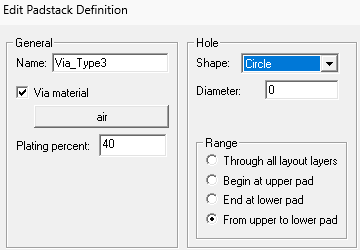
The figure below shows the definition of the via's Percent Platingvalue in the Edit Padstack Definition dialog box.
The weighted average material properties are calculated for each grid cell based on the metal fraction of the cell and the properties of the constituent conductor and dielectric materials. For cells containing vias, the material properties are calculated as described in the preceding note.
The same method as shown in Eq. 1 for thermal conductivity is used to determine the average of all other applicable material properties. Simply substitute the desired property for k. The applicable material properties depend on the solution type, as follows:
- For Thermal Solutions:
- Thermal Conductivity (k)
- Mass Density (ρ) – Relevant only for transient solutions
- Specific Heat (c) – Relevant only for transient solutions
- For Structural Solutions:
- Young's Modulus (E)
- Poisson's Ratio (ν)
- Mass Density (ρ) – Though this property is provided to the solver, in the absence of gravity, acceleration, or rotational velocity excitations (currently unsupported), the material's mass density is not relevant to linear static structural solutions.
- Shear Modulus (G)
- Thermal Expansion Coefficient (α)
Finally, the weighted average material properties are mapped from the grid cells to the elements comprising the model mesh.