
Resistance
The resistance boundary is available for use in DC Conduction solutions. A resistance boundary models a very thin layer of resistive material (such as that caused by deposits or oxidation on a metallic surface) on a conductor at a known potential. Use this boundary condition when the resistive layer’s thickness is much smaller than the other dimensions of the model.
For instance, in the following example, the resistive layer on the conductor is 5x10⁻⁶ meters thick. Since this is four orders of magnitude smaller than the dimensions of the model, use a resistance boundary on the conductor to avoid having to create a very thin object modeling the layer — which could cause problems when the Maxwell generates a mesh for the model and solves for its conduction currents.
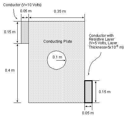
Specify the thickness and conductivity of the resistive material, and the potential of the conductor. Apply resistance boundaries only to the outside edge of the problem space. The external region touching a resistance boundary is assumed to be a PEC (perfect conductor) with a known potential value that is specified in the resistance boundary setup. For the example above, if the PEC region is included in the design model, solve inside should not be selected to exclude it from the FEM (finite element method) problem domain.