
Substrate Stackup
By default, when a component is placed, Electronics Desktop automatically associates a substrate definition with the CompInstance. Not all components need substrate definitions. If it is present, the Substrate definition are shown in the Substrate property in the CompInstance tab.
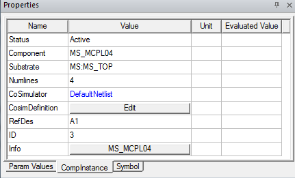
The Substrate property menu shows all defined substrates for this Circuit design. The menu may include the choice <none> to allow changing to a component that doesn’t use a substrate definition (See Using Component Groups). The menu contains the New command which opens the Substrate Definition window.
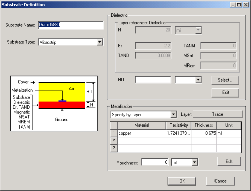
In this window, you have the option of either manually entering data describing the substrate or you can specify the data be taken from layers defined for the layout stackup (See Layout Stackup).
- To manually edit the Dielectric, click Edit.
- To pull data from a dielectric layer, click Select.
- To manually edit the metalization, click Edit.
- To pull data from a metalized layer, change the Trace Metalization drop-down menu to Specify by Layer, then click Layer to select the layer.
Substrate Definitions are all listed in the Project Manager window under the Data folder for the Circuit design.
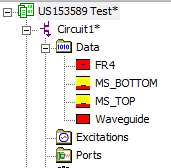
Double-click one of these icons to open the Substrate Definition window and edit the definition.