
Drawing a 2.5D Via in the Layout Editor
- Select a signal or ground layer to draw upon.
- From the Draw menu, select Via.
- Select the center point of the via using the mouse or the keyboard.
- With a via selected, click Draw > HFSS 3D Layout Properties, or right-click the via and select HFSS 3D Layout Properties, which brings up the following drop-down menu:
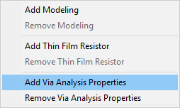
- Select Add Via Analysis Properties to open the EM Design tab of the Properties window.
-
To open the following window, you can also select one or more vias, then right-click the Model/Vias folder in the Project Manager window. Then select Planar EM Properties for Selected Vias.
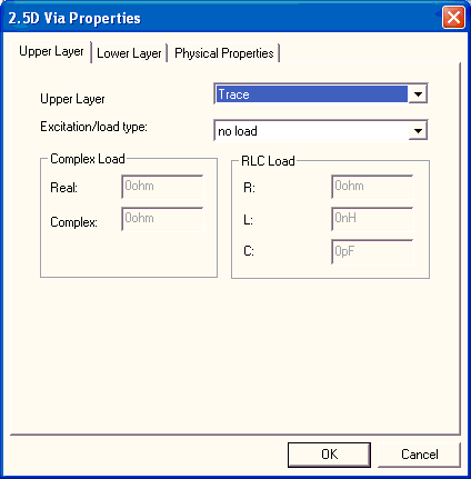
Upper Layer Properties
- Click the Upper Layer tab and do the following:
- Specify the top layer — a signal or ground layer — at which the via terminates.
- If the top layer contains the load, select a load type on the Excitation/Load Type area. You may only define a load at one end of the via. The load on the other end is then set to zero.
- If you selected complex, type the real part of the complex load in ohms in the Real field. Then type the imaginary part of the complex load in ohms in the Complex field.
- If you selected any RLC combination, do the following:
- Type the resistance value in ohms in the R field. It must be a positive or zero value.
- Type the inductance value in nanohenries in the L field. It must be a positive or zero value.
- Type the capacitance in picofarads in the C field. It must be a positive value.
Lower Layer Properties
- Click the Lower Layer tab and do the following:
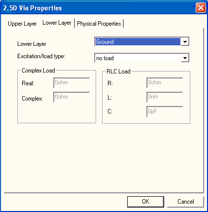
- Specify the bottom layer — a signal or ground layer — at which the via terminates
- If the bottom layer contains the load, select a load type on the Excitation/Load
- If you selected complex, type the real part of the complex load in ohms in the Real field. Then type the imaginary part of the complex load in ohms in the Complex field.
- If you selected any RLC combination, do the following:
- Type the resistance value in ohms in the R field. It must be a positive or zero value.
- Type the inductance value in nanohenries in the L field. It must be a positive or zero value.
- Type the capacitance in picofarads in the C field. It must be a positive value.
Physical Layer Properties
- Click the Physical Properties tab and do the following:
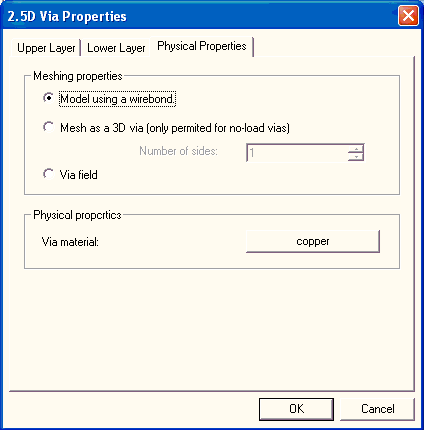
- Optionally, select Model using a wirebond
- Optionally, select Mesh as a 3D Via, then select the number of sides
- Optionally, select Via field
- Click Via material to open the material browser window. Follow the procedure for assigning a material.
- Click OK. The via is set at the specified position.
Note:
When working with a Via, select Draw > Toggle Between Via and Pin to convert the Via to a Pin and then reconfigure the Pin settings using the options described in Creating a Probe Port.