
Creating a Probe Port
In a stripline environment, the additional vertical current that results from using the Reference option to the nearest negative signal may excite the parallel plate mode — which could create inaccurate results.
To create a probe port, you follow much the same procedure for drawing a via, but select coaxialexcitation as the Excitation/load type.
- Select a signal or negative signal layer to draw upon.
- From the Draw menu, select Via.
- Select the via’s center point using the mouse or the keyboard.
- With a via selected, click Draw > HFSS 3D Layout Properties, or right-click the via and select HFSS 3D Layout Properties.
- Select Coax Probe to convert the via to a coaxial probe.
- Select Add HFSS 3D Layout Via to open
the ViaProperties window.
The following controls are available.
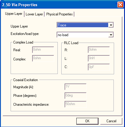
Upper Layer Properties
- Click the Upper Layer tab and do the following:
- Specify the top layer — a signal or negative signal layer — at which the via terminates.
- Select a load type on the Excitation/load type drop-down menu. If the top layer contains the load, select coaxial excitation as the load type. You may only define a load at one end of the probe. The load on the other end is then set to zero.
- If coaxialexcitation is not listed, check whether the coaxial excitation is defined at the other end of the via. If coaxial excitation is not listed at either end of the via, the via needs to be converted to a coaxial probe.
- If you selected complex, type the real part of the complex load in ohms in the Real field. Then type the imaginary part of the complex load in ohms in the Complex field.
- If you selected any RLC combination, do the following:
- Type the resistance value in ohms in the R field. It must be a positive or zero value.
- Type the inductance value in the L field. It must be a positive or zero value.
- Type the capacitance in picofarads in the C field. It must be a positive value.
- Type the chosen current in amps in the Magnitude field.
Generally, use the default value of 1 mA. This specifies the solution’s current is scaled in such a way that the excitation current delivers 1 milliamp. To view the solution at another current, enter a positive value. Only modes with non-zero magnitudes are used in post-processing.
- Type the phase in degrees.
- Type the characteristic impedance in ohms.
Lower Layer Properties
- Click the Lower Layer tab and do the following:
- Specify the bottom layer — a signal or negative signal layer — at which the via terminates
- Select a load type on the Excitation/load type drop-down menu. If the bottom layer contains the load, select coaxial excitation as the load type.
- If you selected complex, type the real part of the complex load in ohms in the Real field. Then type the imaginary part of the complex load in ohms in the Complex field.
- If you selected any RLC combination, do the following:
- Type the resistance value in ohms in the R field. It must be a positive or zero value.
- Type the inductance value in the L field. It must be a positive or zero value.
- Type the capacitance in picofarads in the C field. It must be a positive value.
- Type the chosen current in amps in the Magnitude field.
Generally, use the default value of 1 mA. This specifies the solution’s current is scaled in such a way that the excitation current delivers 1 milliamp. To view the solution at another current, enter a positive value. Only modes with non-zero magnitudes are used in post-processing.
- Type the phase in degrees.
- Type the characteristic impedance in ohms.
Physical Layer Properties
- Click the Physical Properties tab and do the following:
- Model using a wirebond – Vias are modeled as a wirebond; a single wire element connecting the start and end of the via and intersecting all layers in between. This modeling method is recommended when the diameter of the via is electrically small since it is highly accurate and efficient. Vias used in designs that contain 3D structures are automatically modeled as two dimensional ribbons.
- Mesh as a 3D Via — Vias are modeled as a ribbon (sides < 3) or a true three-dimensional solid, depending on the number of sides specified. This modeling method (with sides > 2) can be used for vias of any diameter, but may be inefficient if the via diameter is small.
Number of sides: Defines the n-sided prism to use when meshing the via.
- Via field — For a large number of vias filling a region, the Via field option simplifies the field by thinning the vias within each via cluster on a layer. A cluster is defined as a group of vias with roughly the same inter-via spacing. Thinning does not alter connectivity; all geometry connected by a via remains connected.
Relative min. via spacing: Thinning is based on the minimum average via spacing across all layers. For a regularly spaced array of vias, this value is the via spacing. A value of ‘10’ in this field is interpreted as ’10 via spacings’. For a row of vias, only 1 in 10 vias are used; for an area filled with vias, approximately 1 in 100 vias are used. Since vias are thinned by cluster, and connectivity must be retained, the final pattern of vias may be denser than the requested value.
- Click Via material to open the material browser window. Follow the procedure for assigning a material.
- Click OK. The probe port is listed under Excitations in the Project Tree. Double-click the entry in the Project Tree to edit the probe port’s excitation properties. Additional properties are available in the Properties window.
Individual settings for a via take precedence over the more general settings described. The meshing properties of an individual via are set through HFSS 3D Layout Properties. The HFSS 3D Layout via properties may be removed from a via without removing the via. Older projects may have existing HFSS 3D Layout via properties for all vias. By default, vias no longer automatically receive HFSS 3D Layout via properties.When working with a Probe, select Draw > Toggle Between Pin and Via to convert the Pin to a Via , then reconfigure the Via settings using the options described in Drawing a Via in the Layout Editor.
If a probe port has been defined, all other ports in the model must be gap source ports. You may not combine traditional edge ports, which have de-embedding arms, with probe ports.