
Circuit Ports and Elements in HFSS 3D Layout
Significant simulation speed and efficiency can be gained by using circuit ports and elements in HFSS. You can reduce simulation times by limiting the number of excitations by using circuit elements to include black-box representations directly in HFSS solutions.
Circuit Element Advantages
A circuit port consists of an impressed current source
along with a user-defined parallel impedance load. Compared with traditional ports in HFSS
- The only geometry that must be specified is the location of two terminals.
- A terminal can be defined as a selected edge or as a point touching a metallic object (e.g., an edge port or a point port).
- A design that only contains circuit ports can also be solved at much lower frequencies, compared with using standard ports.
Circuit elements provide a simple and flexible approach to include the effects of lumped circuit elements and allow you to include black box representations as S-parameters directly in an HFSS solution. One benefit of this approach is to reduce the number of excitations required. Reducing the number of excitations reduces the simulation time.
Deembedded Lumped Ports in HFSS 3D Layout are not restricted to being rectangular, they can be arbitrary in shape. A typical non-rectangular lumped port are trapezoidal, with parallel sides connecting to the terminal and its reference. But more complicated shapes are allowed.
A circuit element connection is modeled as if there is actual geometry carrying a conduction current but without the explicit need to define the geometry. This is important to keep in mind since there is an actual connection between two terminals being enforced at the discretized FEM system matrix, and that connection is being solved. Which is similar to the solution if there existed explicit geometry to model that connection. Similar to circuit ports, the only geometry that must be specified is the locations of the terminals defining the circuit connections where each terminal is defined as a selected edge of a metallic object.
Restrictions and Workarounds
The only restriction on the placement of circuit elements and ports is there may not be any gap or wave ports located directly between the terminals of the circuit element/port. While adding a circuit element/port to a design does not explicitly add any conductive material between the terminals, it does add a current path which interferes with any gap or wave ports in between. Such intersections are usually an unintended consequence of using a highly conductive circuit element to add a current return path to a design and can usually be avoided by one of four methods:
- The intersecting wave ports or gap ports can be switched to circuit ports.
- The circuit element can be re-routed by moving the terminals.
- Two separate circuit elements can be used to connect the terminals to a common ground plane or an explicit return path in a separate signal layer.
- If the intersecting ports are horizontal gap ports in a signal layer with non-zero thickness, they can be switched to align with the upper surface of the layer.
HFSS SoD
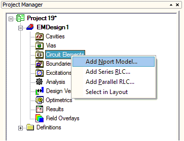
HFSS SoD supports simulation of two-port models, as well as Parallel and Series RLC ideal components. Additionally, HFSS 3D Layout can simulate N-port models. The HFSS solver models two terminal circuit elements by assuming a constant impressed current between the two terminals. HFSS 3D Layout also assumes this current has no radiative coupling to the structure. These assumptions are valid when the separation between the two terminals is electrically short, which is typically the case for such devices as surface mount resistors and capacitors. To add one of these components, right-click 'Circuit Elements' and select 'Add Nport Model', 'Add Series RLC' or 'Add Parallel RLC'.
Select Import Component Mapping File or Import Component File.
- Import Component Mapping File opens a window to select a *.dat partmap file. HFSS reads the partmap file and create (or re-assign) and orient circuit-elements for given components.
- Import Component File opens a window to select a *.cmp file. HFSS reads this cmp file and create (or re-assign) circuit-elements.
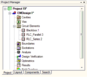
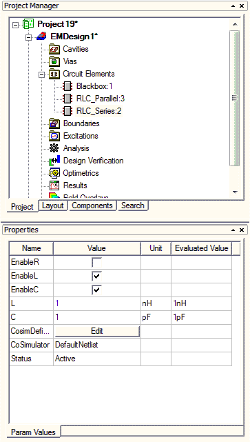
Once circuit elements have been added to an HFSS 3D Layout they appear under the Circuit Elements tree item.
Properties of the RLC components can be edited in the properties window and R, L and C can be deactivated.
Components that do not have footprint geometry are initially rendered on the Symbol layer. When the component is first wired to an object on a physical layer, it renders on that physical layer. For more information see Components with a Symbol Footprint.